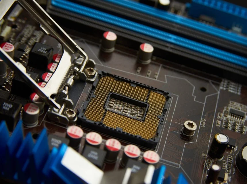
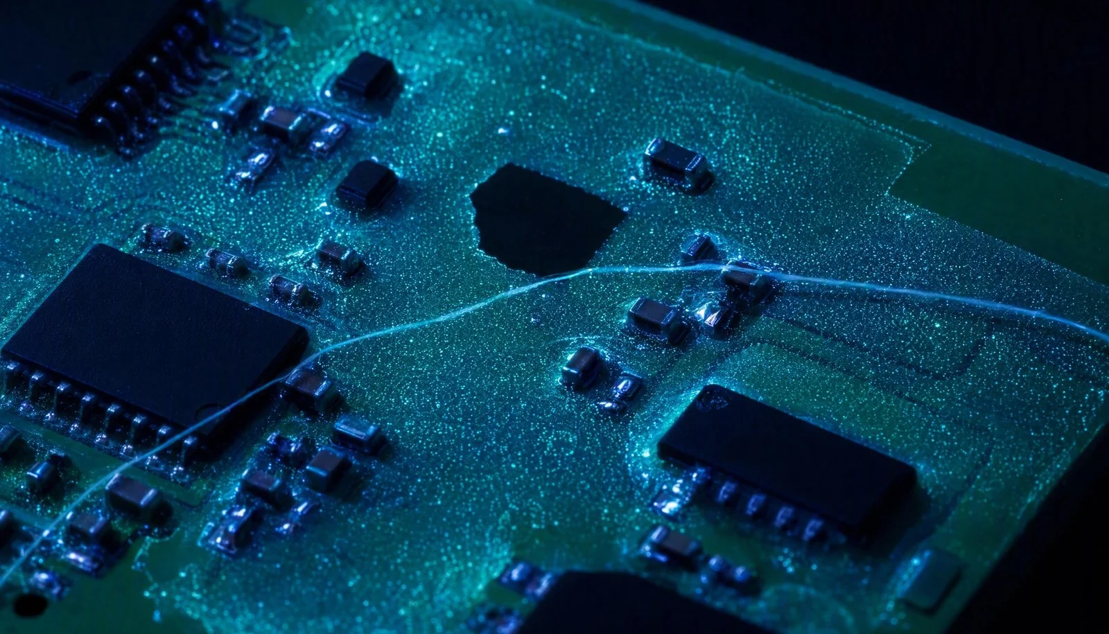
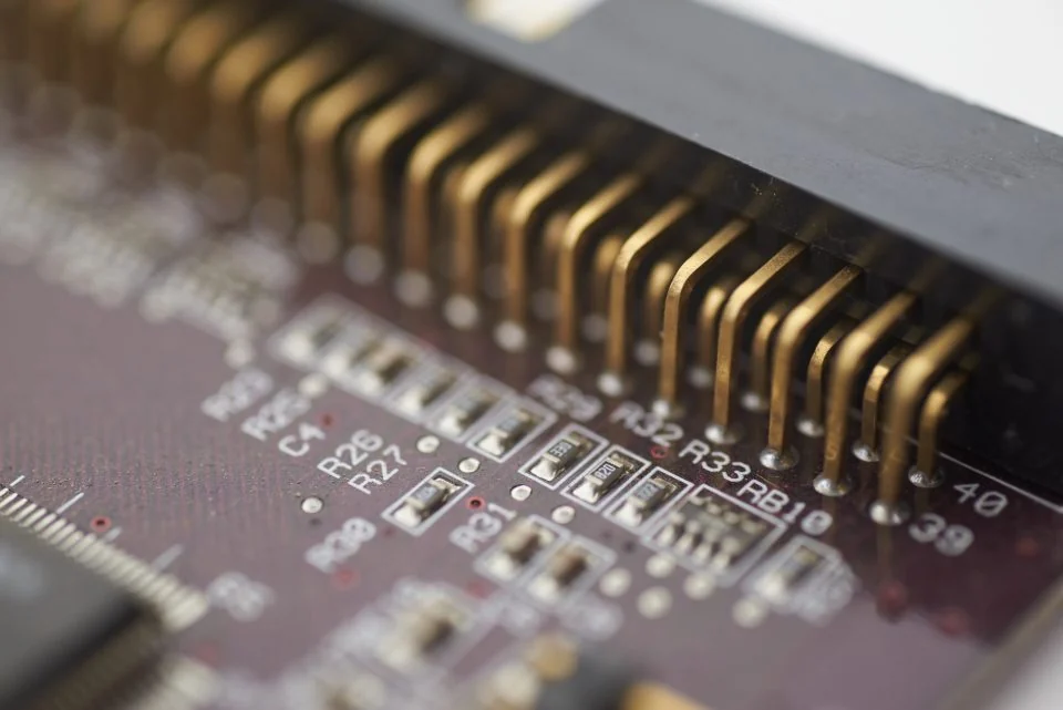
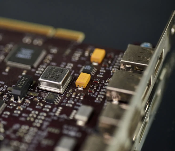
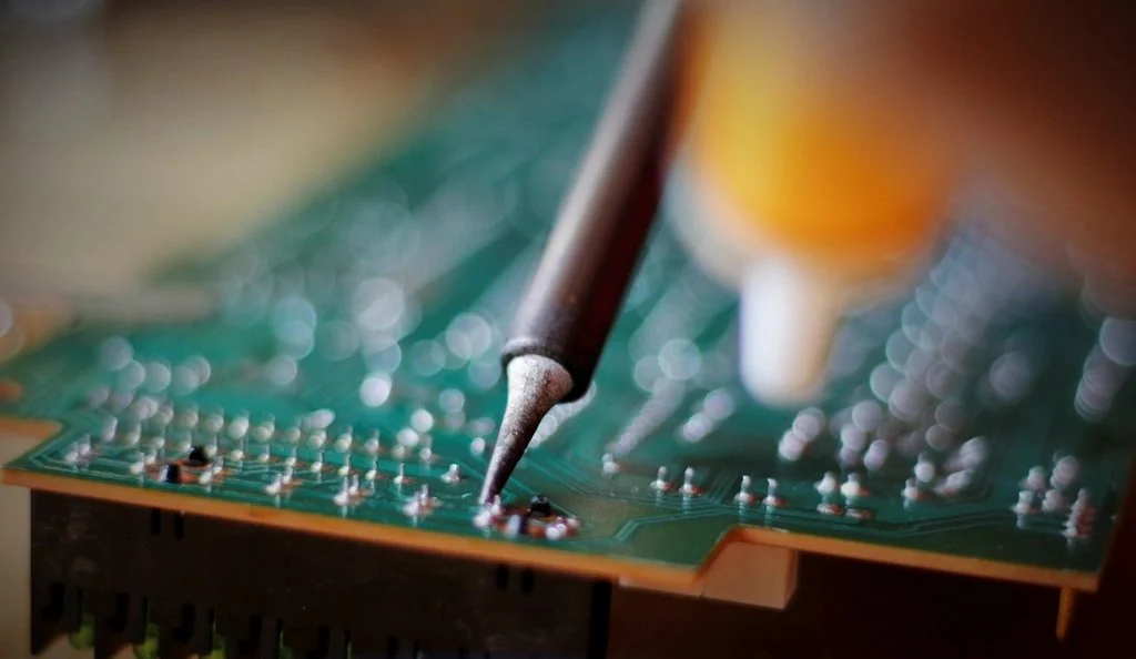
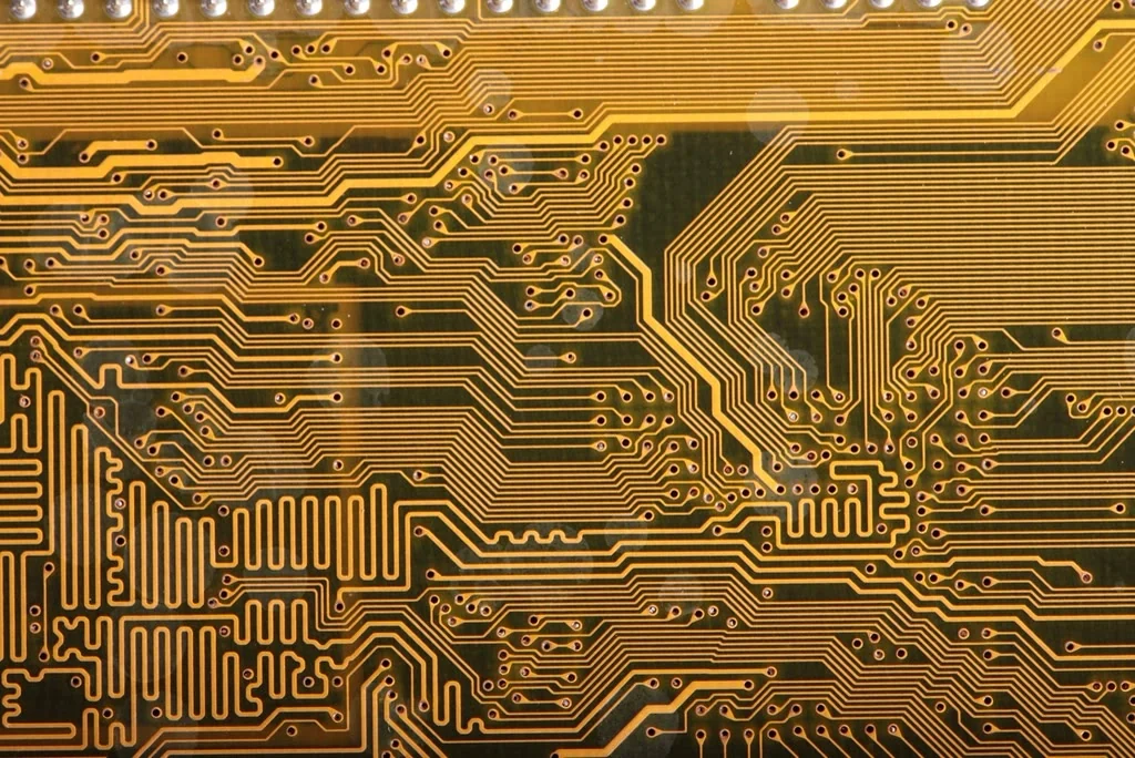
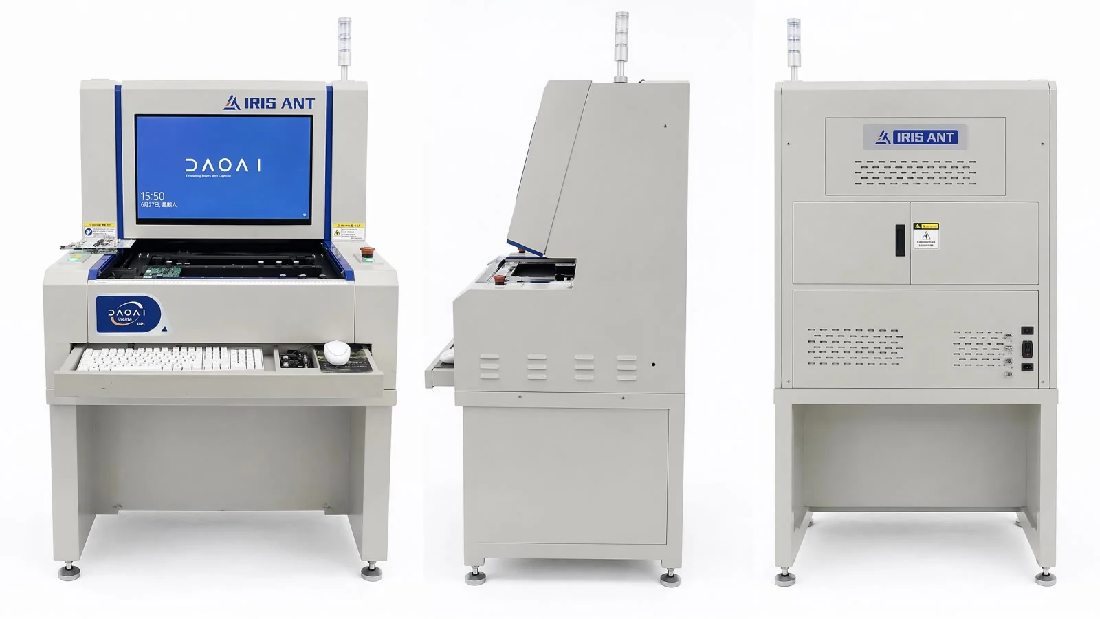
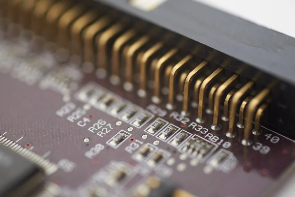
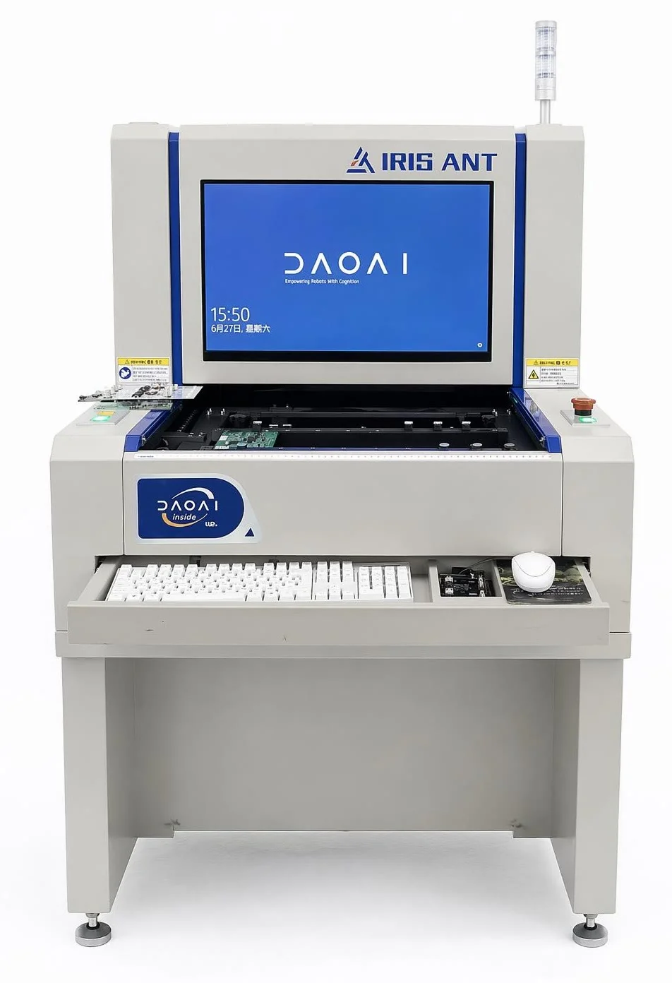
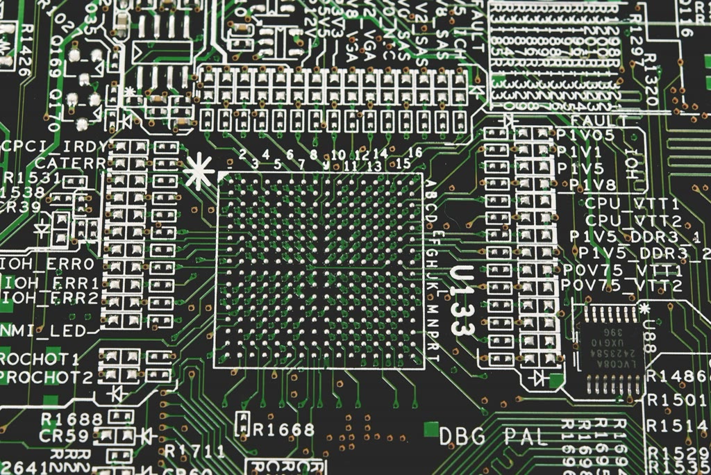
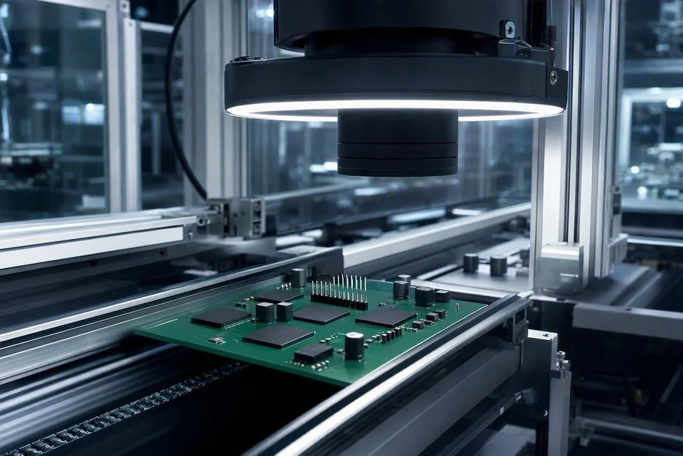
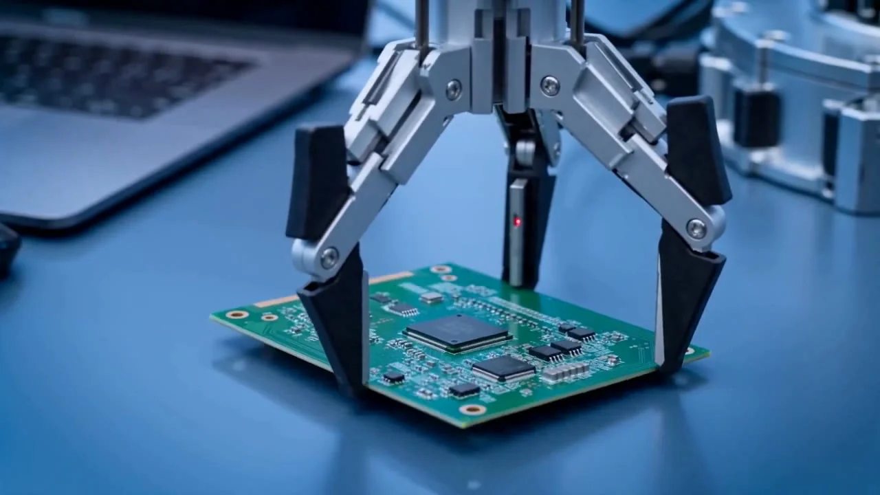
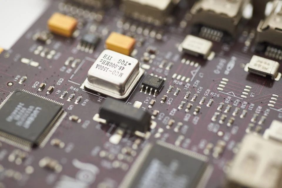
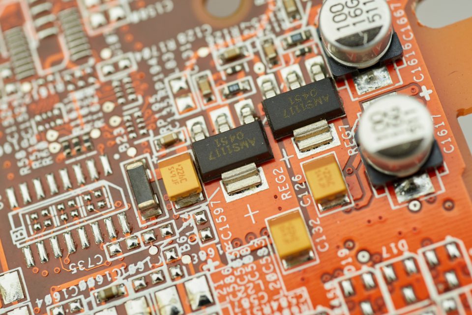
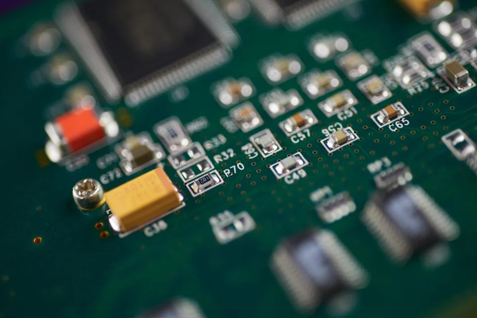
Full-board inspection of SMT, DIP, solder joints and component placement.
Hidden BGA / QFN solder joints: 3D ACI (AI-AOI) images through the package — voids and bridging detected at 99%+ combined accuracy.
Post-reflow false-call reduction: an AI second gate plus APDT positive-sample learning cuts false calls by 80%, with re-inspection workload down 80% too.
Micron-level defects like MLCC micro-cracks: goes live with just 1–20 good samples — no defect library to build first.
High-cadence full assembly inspection: connectors, jumpers and heat sinks checked for missing/mis-assembly, 100% online, with no line-speed penalty.
On electronics and PCBA lines the problem is rarely that the camera cannot see. It is that three things hold at once: defect sizes span three orders of magnitude, defect samples are scarce, and the line speed leaves no room for manual re-checks. BGA and QFN joints sit underneath the package, where 2D optics cannot reach. MLCC micro-cracks are micron-scale, and human judgement of them drifts. At final assembly, connectors, jumpers and heat sinks have to be checked on every board without slowing the line.
Conventional AOI writes the criterion as rules: thresholds, templates, comparison windows. Loose rules miss defects; tight rules raise false calls, and the line falls back on operators to sort them out. That re-inspection station, not the inspection itself, becomes the real capacity bottleneck. With high-mix, low-volume boards, the whole rule set has to be retuned at every changeover.
2. How the solution is put together
Four layers: imaging, model, platform, line integration.
Imaging: 2D covers the whole board at speed; 3D structured light covers height and coplanarity. Voids, bridging, tombstoning and coplanarity deviations are height problems, so they are solved in 3D, with X-ray kept for adjudicating hard cases.
Model: APDT positive-sample learning trains on good boards only — 1–20 good samples are enough to go live, with no defect library to build first. Instance segmentation marks where the defect is, so the result feeds process tracing rather than just an OK/NG flag.
Platform: DaoAI World handles labelling, training, deployment and OTA in the browser. Operator re-checks flow back as training signal, and the model updates in minutes.
Line integration: results, defect images and coordinates are returned to your existing MES / SPC. Production data stays inside the plant.
Where a conventional AOI is already installed, the usual route is a second gate: leave the existing machine untouched, feed the boards it calls NG into the AI for a second judgement, and pass only real defects to a person. It is the smallest change to the line, and the fastest way to bring false calls and re-inspection volume down.
3. Choosing the configuration
Your line today
Recommended
What it addresses
Conventional AOI in place, heavy false calls
AOI software (second gate)
Fewer false calls, re-inspection station freed, existing machine untouched
Full-board SMT inspection, cadence first
2D ACI system
Missing, wrong, shifted components; polarity and silkscreen characters
BGA / QFN, coplanarity, joint height
3D ACI system
Voids, bridging, non-wetting under the package; tombstoning and coplanarity
High-mix, low-volume, frequent changeovers
2D / 3D plus platform templates
Changeover in 5 minutes with no code, no rule rewrite per board type
4. How deployment runs
DaoAI's deployment runs in four steps. ① Assessment — agree the defect types, the cadence and the decision boundary, including what counts as process tolerance rather than a defect. ② Configuration — match systems and stations to board type and cadence, with a quote and a delivery plan. ③ On-site deployment — one good board programs the system automatically in 30 seconds to 5 minutes; operators are up to speed in about 30 minutes. ④ Feedback — re-inspection results flow back and the model updates in minutes.
5. What to measure afterwards
Four numbers are enough: false-call rate, escape rate, re-inspection hours and changeover time. Across DaoAI's deployed electronics / PCBA lines the typical picture is a 80% drop in false calls, re-inspection volume down 80% with it, escapes below 1%, 99%+ combined detection on hidden BGA / QFN joints, and changeovers finished within 5 minutes.
Figures are the typical range our solution reaches in anonymised industry scenarios. Actual values vary with board type, defect class and line cadence; on-site measurement governs.
From SMT solder joints to hidden BGA balls and micro-cracks in passives — ACI drives false calls down while still catching the hard-to-see defects.
Scene · post-reflow SMT
A leading PCB plant · taming post-reflow AOI false calls
ChallengeConventional AOI flags many good boards as defects; operators re-judge image by image and burn review capacity.
SolutionACI as a second gate plus APDT positive-sample learning separates true from false defects by learning only good units — 5-minute, no-code changeover.
−80%False calls
<1%missed escapes
−80%Re-review
Scene · hidden BGA/QFN joints
An automotive-electronics PCBA plant · joints beneath the package
ChallengeBGA/QFN joints hide under the package where optical AOI cannot see; voids and bridges are hard to judge reliably.
Solution3D ACI hardware plus the world model spots voids, bridging and non-wetting in low-contrast imagery.
99%+Detection
3DHidden joints
100%Inline 100%
Scene · MLCC micro-cracks
A passive-component maker · MLCC surface & micro-cracks
ChallengeMLCC micro-cracks and electrode misalignment are micron-scale; manual reading is fatiguing and inconsistent, and defect samples are scarce.
SolutionAPDT positive-sample learning goes live on 1–20 good units, with micron-grade precision and instance segmentation for exact localisation.
1–20Good samples
μmMicron-grade
msPer part
Cases are anonymised industry scenarios; the figures are typical ranges achievable with our solutions.
In-depth cases · IN-DEPTH
Electronics / PCBA · in-depth cases
Each case breaks down the path to deployment in a real scenario — industry context, pain points, our solution and the results.
What defects can AI visual inspection detect in electronics and PCBA?
It covers post-SMT solder defects (insufficient solder, bridging, shift, tombstoning), missing and wrong components, reversed polarity, hidden BGA / QFN joints and MLCC micro-cracks. DaoAI uses a vision foundation model to catch these subtle, low-contrast defects while keeping false calls low.
How does DaoAI's ACI reduce false calls on SMT lines?
It adds an AI second-pass gate after traditional AOI, re-judging suspect points with deep learning. This cuts false-call rework volume by over 70 percent without missing true defects, freeing up inspectors.
What is needed to inspect hidden joints under BGA and QFN packages?
DaoAI 3D ACI reconstructs 3D topography to inspect hidden joints and coplanarity under BGA / QFN devices, covering blind spots that 2D optics cannot see through.
With frequent product changeovers, is AI inspection slow to set up?
No. DaoAI software auto-programs in five minutes from a single good sample, with no CAD and no defect library needed, and reuses quickly across changeovers, ideal for high-mix, low-volume electronics.