INDUSTRY

Semiconductor / Chips

From wafer to advanced packaging — micron-level device-appearance and character inspection.

Semiconductor wafer defect detection
Back to Industries

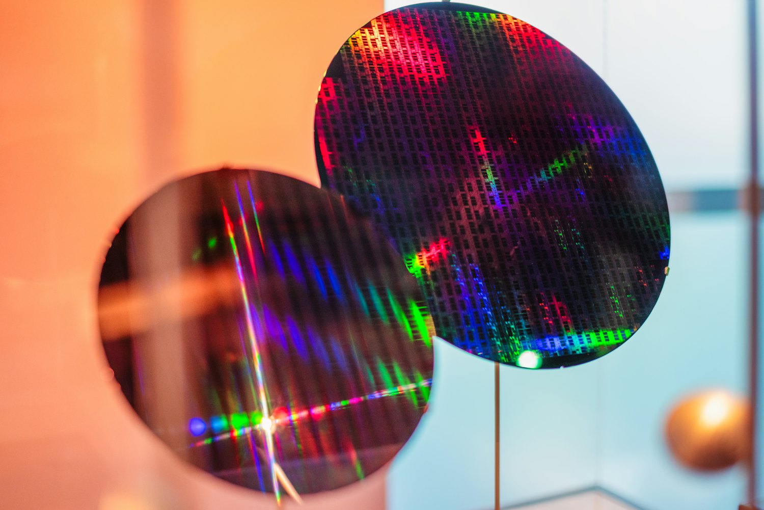
Wafer, advanced-packaging, device-appearance and OCR inspection.

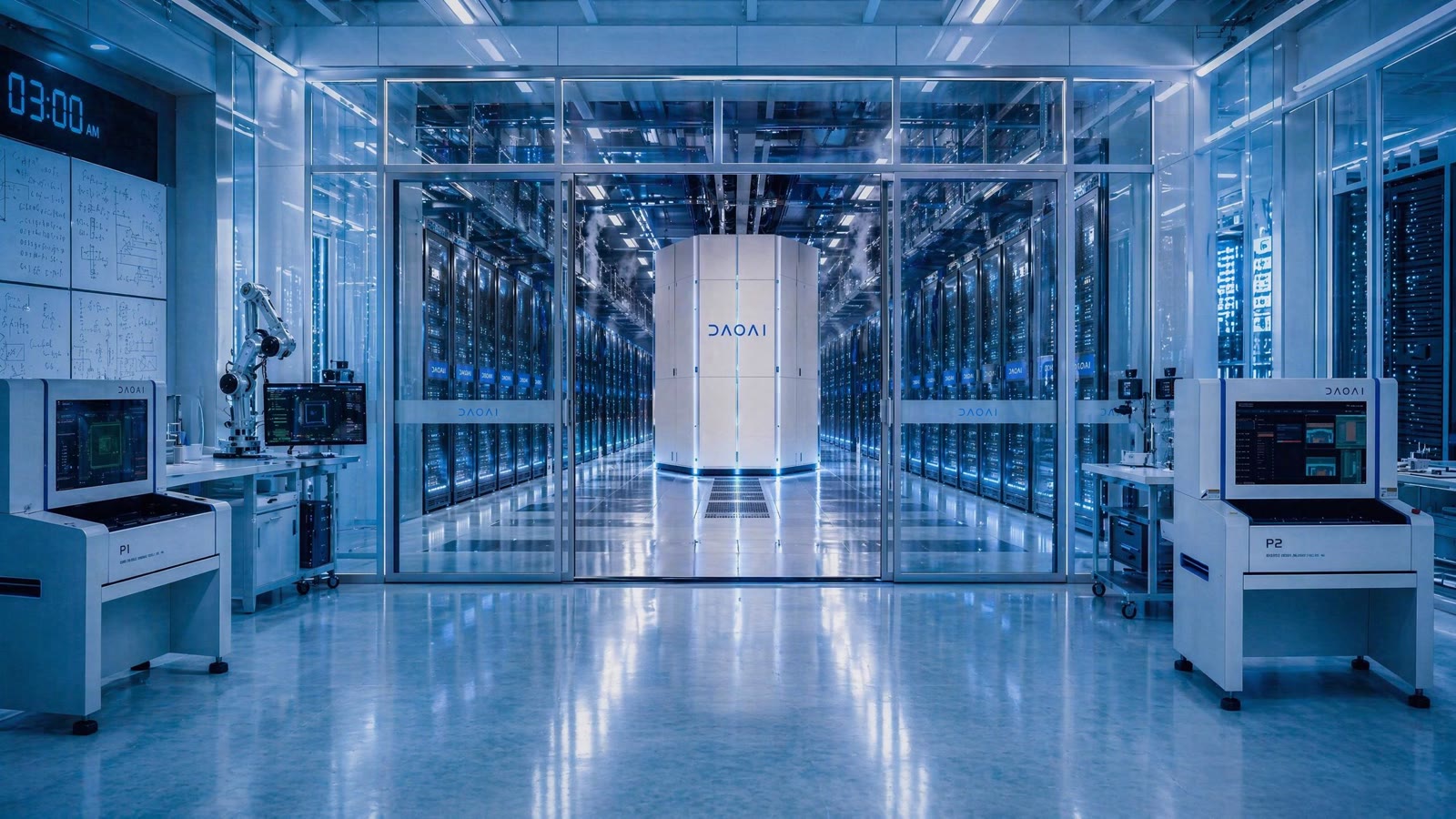
  • Feedback from real lines and real scenes can't be bought.

  • Eight years on the floor, line by line — hard-won engineering experience.

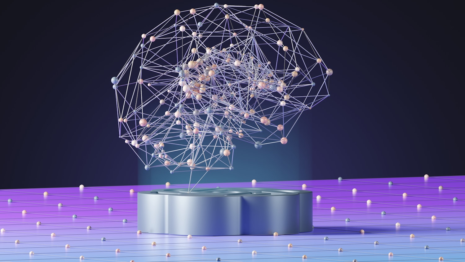
  • Full-stack in-house — the whole chain from sensor to world model is ours.

  • 100M+ real industrial data points continuously refine one world model.

Key checks · KEY CHECKS

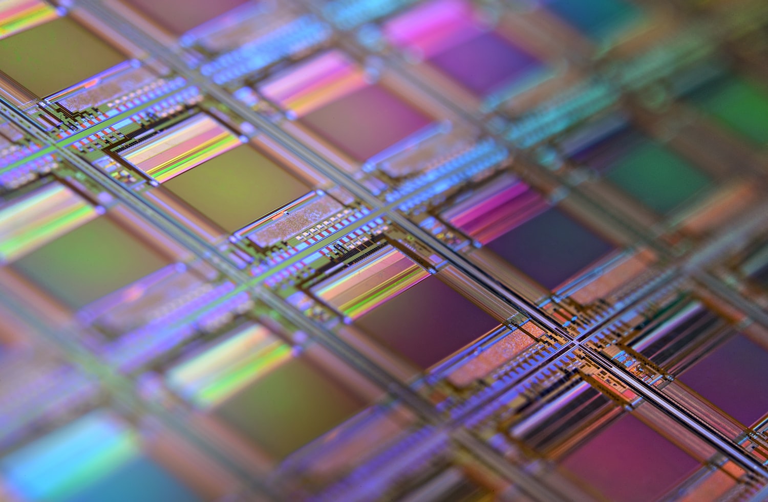
Wafer surface: scratches / particles / chippingLithography & develop defectsWire bonding / gold-wire inspectionPackage cracks & delaminationDie-attach offsetCharacter & mark recognition

Recommended systems: 3D AI AOI · AOI software

Book a Demo Explore Products

Case studies

Semiconductor / chips · wafer to package

From wafer auto-classification to wire-bond and advanced packaging — overkill goes down and defect escapes go to zero.

Scene · wafer ADC

A wafer fab · post-AOI auto defect classification

ChallengeConventional AOI overkill exceeds 20%; cleanroom re-judging is manual, scrapping good dies and inflating labour cost.

SolutionAI-ADC sorts true defects from nuisance; 3D AI-AOI plus the world model generalises across many defect classes.

<2%Overkill
−90%Man-to-machine
+30%Throughput

Scene · post wire-bond

A packaging house · post-bond inspection

ChallengeBond defects such as depressed wires cause major downstream failures if they escape; manual re-judging is low-throughput.

SolutionAI defect classification runs at the edge inside the AI-AOI machine, replacing image-by-image manual review.

98%Accuracy
×2Throughput
→0Escape rate

Scene · rare defects, few-shot

An advanced-packaging plant · covering rare defects fast

ChallengeAdvanced packaging keeps spawning new defect types; none have enough samples and traditional CNNs struggle to cover them.

SolutionAPDT positive-sample learning plus the DaoAI World model generalises to rare defects from only a handful of samples.

Few-shot
>96%Classification
~0.2%Escape rate

Cases are anonymised industry scenarios; the figures are typical ranges achievable with WeLinkirt DaoAI solutions.

In-depth cases · IN-DEPTH

Semiconductor / Chips · in-depth cases

Each case breaks down the path to deployment in a real scenario — industry context, pain points, the DaoAI solution and the results.

Semiconductor wafer defect inspection Semiconductor · 2026-06-16

Post-AOI Wafer Defect Auto-Classification: From Manual Review to AI-ADC

A wafer fab relied on manual AOI review with an overkill rate above 20%. With DaoAI AI-ADC, overkill dropped below 2%, review headcount fell 90%, and line throughput rose 30%.

Read more
Semiconductor chip laboratory inspection Semiconductor · 2026-06-14

Post-Wire-Bond Inspection: Defect Models Pushed to the AI-AOI Edge

A packaging plant relied on manual visual inspection for post-bond defects like sagging wires, with occasional escapes. DaoAI embedded the defect model into the AI-AOI edge device: 98% accuracy, doubled throughput, near-zero escapes.

Read more
Semiconductor chip manufacturing AOI Semiconductor · 2026-06-12

Rare Defects in Advanced Packaging: Few-Shot APDT Positive-Sample Learning

At an advanced packaging plant, new-process defect samples were too scarce for conventional supervised models. DaoAI combined APDT positive-sample learning with world-model generalization: rare-defect classification above 96%, escapes around 0.2%.

Read more
DaoAI World foundation model neural network concept Semiconductor · 2026-06-10

Advanced Packaging Bump Inspection: 3D AI-AOI Catches Missing Bumps and Bridging at Micron Level

At an advanced packaging plant, micro-bump missing and bridging were hard to separate by 2D grayscale. DaoAI 3D AI-AOI judges bump topography from micron-level height data, sharply improving missing and bridging detection.

Read more
AI compute server room infrastructure Semiconductor · 2026-06-08

Lead Coplanarity and Dicing Chipping: 3D Vision Measures Height Per Lead

At a packaging plant, lead coplanarity and dicing chipping were hard to quantify in 2D. DaoAI 3D vision measures height per lead and checks chipping per edge, cutting both coplanarity escapes and chipping misses.

Read more

FAQ

Semiconductor / Chip · AI Visual Inspection FAQ

What defects can AI vision detect in semiconductor manufacturing?

These include wafer surface scratches and particles, wire-bond quality, dicing chipping, missing or bridged bumps, coplanarity, and automatic defect classification (ADC) of rare defects. DaoAI stays stable under low-contrast, high-resolution conditions.

Rare defects are hard to collect, how can AI be trained with few samples?

DaoAI supports few-shot and unsupervised anomaly detection, modeling from good units or very few defect samples, and can flag never-before-seen rare defects as anomalies.

Can automatic defect classification (ADC) replace manual review?

Largely, yes. DaoAI ADC auto-classifies and grades defects, sharply reducing manual review so engineers focus only on a few high-risk categories, improving SPC decisions.

High-resolution inspection generates large data volumes — can it be deployed on-premise to protect process IP?

Yes. DaoAI supports fully on-premise deployment, keeping models and wafer data inside the fab to meet strict process-IP and compliance requirements.