In semiconductor chip production, the inspection of pin coplanarity and dicing chipping is crucial. Traditional inspection methods have many problems, and WeLinkirt provides an effective solution using advanced AI vision technology.
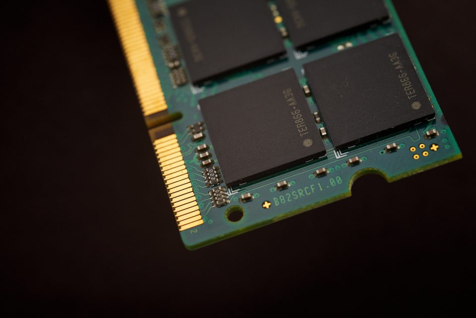
User scenario: The packaging production line of a leading semiconductor chip manufacturer, whose main products are various high - performance chips. In the packaging process, it is necessary to detect the coplanarity of chip pins and the chipping after dicing. The coplanarity of chip pins directly affects the connection stability between the chip and the circuit board, while dicing chipping may cause cracks on the chip edge, affecting the electrical performance and service life of the chip.
Pain points: Traditional detection methods mainly rely on manual visual inspection and simple mechanical measurement, which have many quantitative dilemmas. Manual visual inspection is inefficient, with high labor costs, and is prone to missed detections and false alarms. The missed detection rate is about 3%, and the false alarm rate is as high as 15%. At the same time, the manufacturer produces a wide variety of chips in small batches. When changing models, it is necessary to reprogram and debug, and the downtime is as long as 30min, seriously affecting the production capacity.
Technical principle
WeLinkirt uses advanced AI algorithms and self - developed 3D camera technology to solve these problems. In terms of imaging, the self - developed 3D camera can capture the three - dimensional morphology information of chip pins and dicing areas, providing high - precision data for subsequent detection. In terms of algorithms, it uses the feature recognition ability of the visual basic model to learn and analyze the normal and defective features of chips. Through APDT positive sample/few - sample learning, only 10 good samples are needed for effective model training. At the same time, the semantic false alarm filtering algorithm can screen the detection results and remove false alarms caused by factors such as background interference. The combination of these technologies makes the detection more accurate and efficient. The rich information provided by the 3D camera allows the algorithm to understand the state of the chip more comprehensively, while few - sample learning and false alarm filtering improve the generalization ability and practicality of the model.
- The self - developed 3D camera obtains three - dimensional morphology information to improve detection accuracy.
- The visual basic model learns chip features to achieve accurate recognition.
- APDT few - sample learning reduces the sample requirement and shortens the training time.
- The semantic false alarm filtering algorithm reduces the false alarm rate.
WeLinkirt solution and products
WeLinkirt provides the DaoAI AI AOI software system and the DaoAI 2D / 3D AI AOI equipment. The DaoAI AI AOI software system has the feature recognition ability of the visual basic model, which can realize automatic programming of one good product in 5min with 0 code. Through APDT positive sample/few - sample learning, an accurate detection model can be quickly established. At the same time, the semantic false alarm filtering function can effectively reduce the false alarm rate. The DaoAI 2D / 3D AI AOI equipment uses a self - developed 3D camera, which can perform three - dimensional morphology reconstruction and accurately detect hidden solder joints, coplanarity, and micron - level morphology. In the implementation, the equipment is installed on the packaging production line, and the software system is used for model training and parameter setting to achieve real - time detection of chip pin coplanarity and dicing chipping.
WeLinkirt's AI vision solution brings a new, efficient and accurate experience to semiconductor chip detection.
Quantitative results: By using WeLinkirt's solution, the detection effect of the manufacturer has been significantly improved. The detection rate has increased to 98%, the missed detection rate has decreased to <2%, and the false alarm rate has decreased by −70%. At the same time, the model change time has been shortened from the original 30min to 5min, greatly improving the production capacity.