
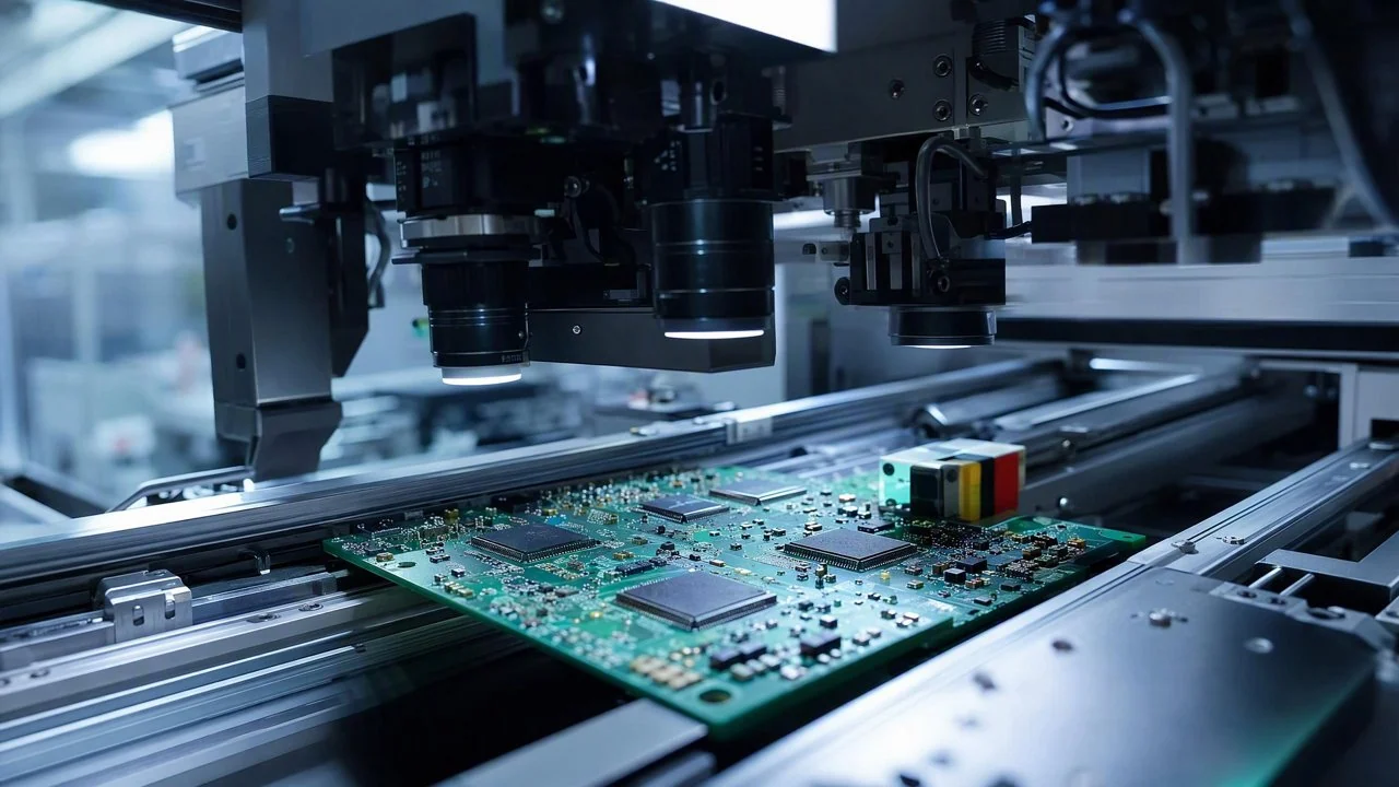
DaoAI 3D AI AOI equipment (featuring self-developed 3D cameras + 3D morphology reconstruction/point clouds, capable of detecting hidden solder joints, coplanarity, micron-level morphology, pores, and other 2D optical blind spot defects, with 2D-3D fusion) leverages deep learning and precise 3D imaging technology. It successfully reduced the omission rate of hidden solder joints in BGA/QFN packages from the traditional 2-3% to an actual production line performance of <0.4%, effectively resolving long-standing quality control challenges in the electronics manufacturing sector.
In the electronics manufacturing industry, particularly in PCBA assembly, the trend towards high-density integration and miniaturization has led to the widespread adoption of advanced packaging technologies such as BGA (Ball Grid Array) and QFN (Quad Flat No-lead). While these packaging forms significantly enhance integration, they also pose challenges that traditional 2D optical inspection solutions struggle to address, especially concerning the quality inspection of hidden solder joints beneath the package body. A mid-sized PCBA manufacturer, whose core business is providing high-reliability circuit boards for telecommunications equipment and industrial control sectors, faced stringent requirements for BGA/QFN device soldering quality. After reflow soldering, these solder joints are concealed beneath the package, making it impossible to effectively determine defects like opens, shorts, voids, or cold joints using only 2D images. This situation led to high product reliability risks.
Pain Points: Why This Hurdle Was So Difficult
Under traditional inspection methods, this manufacturer experienced an omission rate for hidden BGA/QFN solder joints as high as 2-3%, severely impacting production yield and customer satisfaction. The inability to detect these potential defects at an early stage meant issues only surfaced during subsequent functional testing, leading to exorbitant rework costs. Some defects even went undetected until products reached end-users, resulting in significant brand reputation damage and recall risks. Manual re-inspection of these complex defects was labor-intensive and inefficient; a skilled quality inspector could only process a limited number of BGA/QFN defect re-inspections daily, making misjudgments due to fatigue highly probable. Furthermore, with product iterations and diverse packaging types, traditional rule-based AOI systems suffered from lengthy changeover times, with each new product introduction requiring several hours or even half a day for programming and debugging, severely restricting the production line's flexibility.
The root cause of these difficulties lies in the structural characteristics of BGA/QFN packages. Solder balls or pads are completely obscured by the chip body, forcing traditional 2D optical AOI to rely on indirect judgments based on solder overflow at the pad edges or side shadows. This method is highly susceptible to variations in lighting, angle, and minute solder volume fluctuations, leading to high false positive and omission rates. For example, insufficient solder might be mistakenly identified as an open circuit, when in reality, it's merely insufficient solder height, or solder collapse might be misidentified as a short. Moreover, micron-level defects like pores and internal voids within solder joints are absolute blind spots for 2D imaging. These challenges are similar to those in AI quality inspection for apparel manufacturing, where smart scheduling optimization and efficiency improvement are achieved through multi-model collaboration. Both scenarios demand precise identification and efficient processing of multi-dimensional, complex, and hidden information, along with strong generalization capabilities and rapid adaptability to evolving production needs.
Technical Principles
DaoAI's 3D AI AOI equipment fundamentally solves the challenge of hidden BGA/QFN solder joint inspection through its self-developed high-precision 3D cameras and advanced 3D morphology reconstruction technology. The device employs a multi-angle structured light projection combined with point cloud data acquisition, enabling high-resolution 3D scanning of PCB surfaces and components to obtain precise Z-axis height information. By reconstructing a complete 3D model of solder joints, pads, and package bodies from the massive collected point cloud data, the DaoAI AI engine can 'see through' the package. This allows for direct measurement of critical parameters such as the height, volume, coplanarity, shape, and presence of voids in hidden solder joints. This direct 3D measurement method offers unparalleled accuracy and reliability compared to the indirect judgments of traditional 2D AOI. For instance, for BGA solder joints, DaoAI 3D AI AOI can precisely identify and measure solder ball height consistency, diameter, collapse degree, and even tiny internal voids, which are crucial details unavailable from 2D images. Actual production data shows that DaoAI 3D AI AOI equipment consistently maintains a detection rate of over 99.6% for hidden BGA/QFN solder joints in typical PCBA production environments.
Compared to traditional rule-based AOI, the core advantage of DaoAI 3D AI AOI equipment lies in its deep learning AI algorithms. Traditional rule-based AOI relies on manually defined, complex rule sets, which struggle to cover the diverse optical characteristics and minute defects of BGA/QFN solder joints, leading to high false positive rates. In contrast, the DaoAI AI AOI software system uses APDT (Adaptive Pre-trained Deep Learning) few-shot self-training technology, requiring only 1-20 good samples to quickly learn normal solder joint morphological features and automatically identify various anomalies. This feature-recognition-based learning approach enables the system to effectively distinguish true defects from process variations, significantly reducing false positives. Furthermore, the 2D-3D fusion detection capability allows DaoAI 3D AI AOI equipment to handle both 3D morphological defects and leverage the advantages of traditional 2D optical inspection, such as component polarity and character recognition, achieving comprehensive coverage. This multi-modal information fusion and intelligent decision-making mechanism aligns perfectly with the current trend of optimizing and enhancing efficiency through multi-model collaborative work, significantly improving detection robustness and efficiency.
Typical Application Scenarios
- **BGA/QFN Hidden Solder Joint Defect Detection:** This is the core strength of DaoAI 3D AI AOI equipment. Through 3D morphology reconstruction, it directly detects whether solder joints beneath the package body have defects such as opens, shorts, voids, cold joints, bridges, insufficient/excessive solder. The challenge lies in the complete obstruction of solder joints, making direct 2D vision impossible, and the tiny, diverse nature of defects, demanding extremely high precision in 3D measurement.
- **Chip Pin Coplanarity Inspection:** For QFN, QFP, and other leaded packages, pin coplanarity directly affects soldering reliability. DaoAI 3D AI AOI can precisely measure the height difference of all pin ends relative to a reference plane, ensuring coplanarity within allowable tolerances to prevent opens or poor contact due to pin warpage. The difficulty lies in achieving micron-level measurement precision for tiny pins.
- **Micron-level Morphology Defect Detection:** This includes scratches on pads, foreign objects, tiny pits or scratches on the PCB surface, and burrs or solder balls on solder joint surfaces. These defects are typically extremely small and difficult for traditional 2D AOI to reliably detect. DaoAI 3D AI AOI, with its high-resolution 3D imaging, can clearly identify and quantify these micron-level morphological anomalies.
- **Void and Porosity Analysis:** Voids or pores within solder joints reduce their mechanical strength and electrical conductivity. DaoAI 3D AI AOI equipment, through its high-precision 3D data, can identify void characteristics on and within solder joints (inferred from morphological features) and conduct quantitative analysis, a capability impossible with 2D optical inspection.
- **Solder Volume and Solder Joint Volume Measurement:** For various solder joints (including chip component solder joints), DaoAI 3D AI AOI can precisely measure solder volume and height, ensuring solder quantity conforms to process specifications and avoiding reliability issues caused by insufficient or excessive solder. The challenge lies in the complexity of solder morphology for different pad sizes and component types.
Case Study
Before adopting DaoAI 3D AI AOI equipment, a mid-sized PCBA manufacturer relied primarily on traditional 2D AOI combined with X-Ray sampling for hidden BGA/QFN solder joint inspection. Under this traditional approach, production line data indicated an omission rate for hidden BGA/QFN solder joints as high as 2.5%, leading to monthly rework and scrap costs exceeding hundreds of thousands of RMB, alongside frequent customer complaints. To address this pain point, the manufacturer introduced DaoAI 3D AI AOI equipment for online full inspection. During the initial rollout, the DaoAI engineering team collaborated closely with the client, leveraging the APDT few-shot learning capabilities of the DaoAI AI AOI software. Using only 15 good samples, they completed defect model training and validation for various BGA/QFN packages within 3 hours. After a month of pilot operation and data validation, in this case, the DaoAI 3D AI AOI equipment successfully reduced the omission rate of hidden BGA/QFN solder joints to <0.4%. Concurrently, due to the integration of 3D information and the precise judgment of the AI model, the false positive rate also decreased from a previous 8-10% to around 3%, significantly reducing the burden of manual re-inspection. Production line data showed that after implementation, the rework rate due to BGA/QFN solder joint defects decreased by over 60%, and product yield improved by approximately 2.1 percentage points, markedly enhancing production efficiency and product quality stability.
DaoAI 3D AI AOI equipment not only resolved the blind spots in BGA/QFN hidden solder joint inspection but also, through its AI learning capabilities, freed production lines from the troubles of high omissions and false positives, truly achieving intelligent upgrades in quality control.
DaoAI Solutions and Products
The core solution provided by DaoAI to this mid-sized PCBA manufacturer is its 3D AI AOI equipment, which integrates DaoAI's self-developed high-precision 3D cameras and the powerful DaoAI AI AOI software system. At the hardware level, the self-developed 3D camera, through precise optical design and high-speed data acquisition, can capture nanosecond-level 3D point cloud data, ensuring micron-level measurement accuracy. At the software level, the DaoAI AI AOI software system serves as the intelligent brain of the entire solution, built upon advanced visual foundation models with powerful feature recognition capabilities. For hidden BGA/QFN solder joint detection, the system utilizes APDT (Adaptive Pre-trained Deep Learning) technology, requiring only a minimal number (1-20) of good samples for rapid, 0-code automated programming and model training. This means that when the client's production line switches product models, changeover downtime can be reduced from several hours to within 5 minutes, greatly enhancing production line flexibility and efficiency. Furthermore, DaoAI 3D AI AOI equipment supports 2D-3D fusion detection, ensuring comprehensive coverage of all defect types, whether surface defects or hidden morphological defects, can be effectively identified. The entire system supports 100% on-premise private deployment, guaranteeing customer data security and the independence of production processes.
The implementation process of this solution was efficient and transparent. During the modeling phase, the client only needed to provide a few good samples, and the DaoAI AI AOI software system could automatically learn and establish defect detection models. For changeovers, quick adaptation to new products was achieved through simple parameter adjustments and few-shot learning. In terms of deployment and integration, DaoAI 3D AI AOI equipment can be seamlessly integrated into existing SMT production lines, offering various deployment methods such as SDK/API/Docker to meet diverse client integration needs. Additionally, DaoAI provides the DaoAI World model as a unified foundation, ensuring the AI model's semantic understanding and cross-scenario generalization capabilities, enabling continuous learning and optimization from production line feedback to further enhance detection accuracy and efficiency. Through the application of DaoAI 3D AI AOI equipment, this manufacturer not only resolved the challenging problem of hidden BGA/QFN solder joint inspection but also achieved a shift from 'post-event remedy' to 'proactive prevention' in quality management, significantly enhancing its core competitiveness.
FAQ
How does DaoAI 3D AI AOI equipment detect hidden BGA/QFN solder joints?
DaoAI 3D AI AOI equipment utilizes self-developed high-precision 3D cameras to acquire multi-angle structured light data, followed by 3D morphology reconstruction to obtain complete 3D data of solder joints. Combined with the deep learning algorithms of the DaoAI AI AOI software system, it directly analyzes 3D features such as solder joint height, volume, coplanarity, and voids, enabling precise detection of hidden solder joints beneath the package body.
What are the advantages of DaoAI 3D AI AOI equipment compared to traditional X-Ray inspection?
Compared to traditional X-Ray inspection, DaoAI 3D AI AOI equipment offers online, non-contact, and radiation-free advantages, enabling 100% full inspection with faster detection speeds. The few-shot learning capability of DaoAI AI AOI software allows for quicker changeovers, higher cost-effectiveness, and provides richer solder joint morphological details for quality traceability.
What is the budget required to deploy DaoAI 3D AI AOI equipment?
The budget for DaoAI 3D AI AOI equipment is influenced by factors such as configuration (e.g., detection speed, precision, field of view), integration complexity, and selected software function modules. We offer flexible solution customization. We recommend contacting our sales engineers to receive a detailed quotation and ROI analysis based on your specific production line needs and inspection objectives.
Full solution for this scenario: the full inspection solution for 3D AI AOI Equipment · 3D Inspection for Hidden BGA / QFN Solder Joints
This article was generated by AI. Customer cases are simulated scenarios based on real product capabilities and figures are illustrative; see product pages for official benchmarks.