
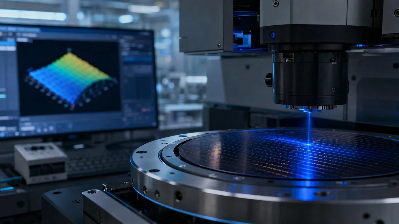
DaoAI 3D AI AOI equipment (featuring self-developed 3D cameras + 3D morphology reconstruction/point clouds, detecting hidden solder joints/coplanarity/micron-level morphology/voids and other 2D optical blind spot defects, with 2D-3D fusion) leverages APDT few-shot self-training to reduce false positive rates for pin coplanarity and dicing chipping inspection from approximately 15% to below 5.2% at a mid-sized chip packaging facility, significantly optimizing semiconductor packaging quality control processes. In the semiconductor industry, precise detection of micron-level defects such as chip pin coplanarity and dicing chipping is crucial for ensuring product reliability. As chip integration increases and package sizes miniaturize, traditional rule-based AOI systems often struggle with complex geometries and varied defect patterns. This is particularly true when introducing new products or after minor process adjustments, which typically demand significant time and human effort for model tuning.
In semiconductor packaging, pin coplanarity is one of the critical indicators of chip package quality. Especially for high-density packages like Surface Mount Devices (SMD) and Ball Grid Arrays (BGA), even slight non-coplanarity of pins can lead to poor soldering, open circuits, or even short circuits, severely impacting subsequent assembly and product reliability. Simultaneously, micron-level chipping defects during wafer dicing can become potential failure points for chips. As high-precision applications like optical module manufacturing demand higher chip reliability, traditional inspection solutions often fall short in efficiency and accuracy when facing these challenges, struggling to meet the rapid iteration demands of production. DaoAI 3D AI AOI equipment is designed to address these pain points, demonstrating exceptional performance in semiconductor packaging pin coplanarity and dicing chipping inspection by combining self-developed 3D cameras with advanced APDT few-shot self-training technology.
Pain Points: Why This Hurdle Is Difficult to Overcome
Semiconductor packaging lines face multiple challenges in pin coplanarity and dicing chipping inspection. First, the precision requirements are extremely high: pin non-coplanarity is typically measured in microns or even sub-microns. Traditional 2D vision systems are limited by the lack of Z-axis information, making it difficult to accurately capture subtle height differences. For example, the industry generally requires pin coplanarity deviation to be less than 0.1mm, with many high-end chips demanding less than 0.05mm, meaning any tiny optical blind spot can lead to missed detections. Second, false positive rates remain high: due to reflective chip surfaces, subtle texture variations, and tiny burrs or residues on diced edges, traditional rule-based AOI systems frequently misclassify normal features as defects. Production line data shows that before adopting new technology, a mid-sized chip packaging facility experienced false positive rates for pin coplanarity inspection as high as 15%, significantly hindering production efficiency and increasing manual re-inspection workload. Finally, model training and changeover are difficult: with a wide variety of chip products and package forms, each product or process adjustment requires retraining the inspection model. Traditional AI models need a large number of defect samples for effective training, but defect samples are scarce in actual production. For new product introductions, model training cycles can take days or even weeks, leading to long production line downtime and impacting throughput and costs. These issues highlight the urgent need for smarter, more efficient, and more flexible inspection solutions, especially when addressing the high-precision defect detection challenges encountered by Gocator 3D vision technology in optical module manufacturing, where the limitations of traditional solutions become even more apparent.
The root causes of these difficulties lie in the physical properties of semiconductor materials and the complexity of micro-scale processes. Silicon wafers and packaging materials have certain optical reflectivity, which can easily cause specular or diffuse reflection at specific angles, leading to overexposure or underexposure in 2D images, masking real defects. At the same time, the microscopic structures of pin metal surfaces and diced edges result in highly irregular defect morphologies. For example, dicing chipping may appear as irregular depressions, protrusions, or delaminations, which are often difficult to distinguish in 2D images. Furthermore, the accelerating production pace demands higher processing speeds from inline inspection systems. Achieving high-speed inspection while maintaining high precision is a core challenge facing semiconductor manufacturing today.
Technical Principles
DaoAI 3D AI AOI equipment effectively solves the aforementioned pain points through its unique combination of technologies. The core lies in its self-developed 3D camera and 3D morphology reconstruction technology. This camera utilizes multi-point laser scanning or structured light projection principles to accurately acquire 3D point cloud data of the measured object's surface, thereby enabling micron-level morphology reconstruction of chip pins and diced edges. Unlike traditional 2D images, 3D point cloud data includes height information, allowing critical parameters such as pin non-coplanarity, dicing chipping depth, and volume to be directly and accurately measured. DaoAI 3D AI AOI systems fuse this 3D data with 2D images, compensating for the Z-axis blind spots of 2D vision while also considering surface texture information.
Furthermore, DaoAI has introduced APDT (Adaptive Positive Data Training) few-shot self-training technology at the AI algorithm level. Traditional AI algorithms often require a large number of annotated defect and non-defect samples for effective training, which is prohibitive in the semiconductor industry where defects are scarce and annotation costs are high. The core of APDT technology is its ability to perform initial learning using only a small number of normal (good) samples, then adaptively identify and learn potential anomaly patterns from subsequent production data. This means that when a new product is introduced or a minor process change occurs, DaoAI 3D AI AOI equipment can complete rapid model adaptation and optimization within minutes, using only 1-20 good samples, without requiring extensive manually annotated defect samples. This few-shot learning capability, compared to traditional rule-based AOI, not only significantly shortens changeover times and reduces reliance on human expertise but also effectively prevents missed detections and false positives caused by insufficient samples. For example, in a practical application at a mid-sized chip packaging facility, this solution reduced new product changeover time from several hours to under 5min, significantly improving production line flexibility and efficiency.
Typical Application Scenarios
- **Pin Coplanarity Inspection:** DaoAI 3D AI AOI equipment accurately measures the Z-axis height of each pin through high-precision 3D point cloud reconstruction, calculating the coplanarity deviation of the pin array. For BGA, QFN, and other package types, it can detect whether pins are within the same plane or if there are bending, warping, or other defects that are extremely difficult to distinguish in 2D images.
- **Dicing Chipping and Crack Detection:** After wafer dicing, the equipment's 3D vision capability accurately captures micron-level chipping, burrs, or cracks on the chip edges. Through in-depth analysis of edge morphology, it effectively differentiates between normal cutting marks and potential structural defects, preventing reduced chip strength or subsequent packaging issues due to chipping.
- **Solder Joint Morphology and Void Detection:** For solder joints in chip packaging, DaoAI 3D AI AOI can inspect solder joint volume, height, wettability, and the presence of internal voids or air bubbles. These defects directly affect the mechanical strength and electrical performance of solder joints, and 3D imaging can penetrate the surface to reveal internal structures.
- **Foreign Object and Contamination Detection:** Combining 2D-3D fusion technology, the equipment can identify tiny foreign objects, particles, or contamination on the chip surface. These foreign objects might be overlooked in 2D images due to insufficient contrast but become more reliably detectable due to height differences in 3D morphology.
- **Package Dimension and Deformation Inspection:** DaoAI 3D AI AOI can also perform high-precision measurements of overall chip package dimensions, flatness, and warpage. This is crucial for controlling package consistency and ensuring a good match between the chip and the circuit board.
Case Study
A mid-sized chip packaging enterprise, specializing in high-reliability chips for optical communication modules and automotive electronics, previously relied on traditional rule-based AOI and manual inspection for pin coplanarity and dicing chipping detection. The traditional rule-based AOI had a high false positive rate, especially after new product introductions or minor process parameter adjustments, where it could reach up to 15%. This resulted in a large number of good products being sent for manual re-inspection. Production line data indicated approximately 30 additional man-hours per day were spent on manual re-inspection, severely slowing down the overall production rhythm. Concurrently, due to the scarcity of defect samples, traditional AI model training cycles for each new product launch extended to several weeks, causing excessive production line downtime. To address these issues, the enterprise introduced DaoAI 3D AI AOI equipment, specifically leveraging its APDT few-shot self-training capability.
In the initial deployment phase, the DaoAI engineering team collaborated closely with the client. The APDT model's initial training was completed within minutes, using only about 10 good samples. In live operation, the system accurately captured micron-level pin non-coplanarity and dicing chipping defects. Production line data shows that after the deployment of DaoAI 3D AI AOI, the false positive rate for pin coplanarity and dicing chipping inspection decreased from approximately 15% to <5.2%, a reduction of over 65%. Simultaneously, the missed detection rate was consistently kept at an extremely low level of <0.4%. Crucially, APDT technology reduced new product changeover time from several hours to under 5min, significantly improving production line flexibility and utilization. In this case, the client's production efficiency significantly improved, manual re-inspection workload was effectively reduced, directly cutting labor costs on the production line, and substantially enhancing the quality of shipped products.
“DaoAI 3D AI AOI's APDT technology has completely transformed our new product introduction process. Previously, our production lines often halted while waiting for model training and tuning. Now, with just a few good samples, the system quickly adapts, which has greatly boosted our production efficiency and market responsiveness.”
DaoAI Solutions and Products
DaoAI's 3D AI AOI solution for the semiconductor industry is centered on its self-developed 3D camera and the DaoAI AI AOI software system. The 3D AI AOI equipment integrates a high-precision 3D imaging module, capable of acquiring complete 3D morphological data for critical areas such as chip pins and diced edges. At the software level, the DaoAI AI AOI software system features the APDT few-shot self-training engine, which enables customers to quickly deploy and iterate inspection models without requiring a large number of defect samples. During the model building phase, users only need to provide a small number of good product images, and the system can self-train via APDT, greatly simplifying the complex process of traditional AI models that require extensive annotated data. Addressing the specific needs of the semiconductor industry, DaoAI 3D AI AOI supports 100% on-premise private deployment, ensuring customer data security and intellectual property protection, while offering various integration methods like SDK / API / Docker for seamless connection with existing MES/SCADA systems. Furthermore, the DaoAI World Model, serving as a unified foundation, provides powerful semantic understanding and cross-scenario generalization capabilities for 3D AI AOI, ensuring the system continuously learns from production line feedback to improve inspection performance.
Through the deployment of DaoAI 3D AI AOI equipment, this mid-sized chip packaging facility achieved multiple business values. Production line data shows that the false positive rate for pin coplanarity and dicing chipping inspection was reduced by over 65%, significantly decreasing manual re-inspection workload. New product changeover time was shortened from several hours to within 5min, increasing production line utilization by approximately 10%. Concurrently, the missed detection rate was consistently maintained below <0.4%, ensuring product quality and reducing the risk of rework and recalls due to escaped defects. These quantified achievements directly translate into substantial cost savings and efficiency gains, helping the client maintain competitiveness in high-precision semiconductor manufacturing.
FAQ
How does DaoAI 3D AI AOI's APDT technology differ from traditional AI training?
The primary difference between DaoAI 3D AI AOI's APDT (Adaptive Positive Data Training) technology and traditional AI training lies in sample requirements. Traditional AI typically needs a large number of annotated defect and good samples for training, whereas APDT can complete initial model training with just 1-20 good samples and continuously optimize through an adaptive learning mechanism. This significantly shortens model deployment and iteration cycles, especially suitable for the semiconductor industry where defect samples are scarce.
What major defect types can 3D AI AOI equipment cover in semiconductor packaging inspection?
DaoAI 3D AI AOI equipment can cover various defect types in semiconductor packaging inspection, including pin coplanarity, dicing chipping, solder joint morphology (including voids/porosity), micron-level foreign objects and contamination, and package dimensions and deformation. Its self-developed 3D camera provides precise 3D morphological data, effectively addressing the Z-axis blind spots of traditional 2D vision, enhancing detection accuracy and coverage.
What is the approximate cost budget for deploying DaoAI 3D AI AOI solution?
The cost budget for deploying DaoAI 3D AI AOI solution varies depending on specific configurations, inspection requirements, complexity of production line integration, and deployment mode (e.g., on-premise private deployment). We offer flexible software and hardware combined solutions that can be customized based on the client's actual situation. We recommend contacting our sales team with your detailed requirements, and we will provide a personalized quote and return on investment analysis to ensure optimal solution.
Full solution for this scenario: 3D AI AOI Equipment industry solutions
This article was generated by AI. Customer cases are simulated scenarios based on real product capabilities and figures are illustrative; see product pages for official benchmarks.