
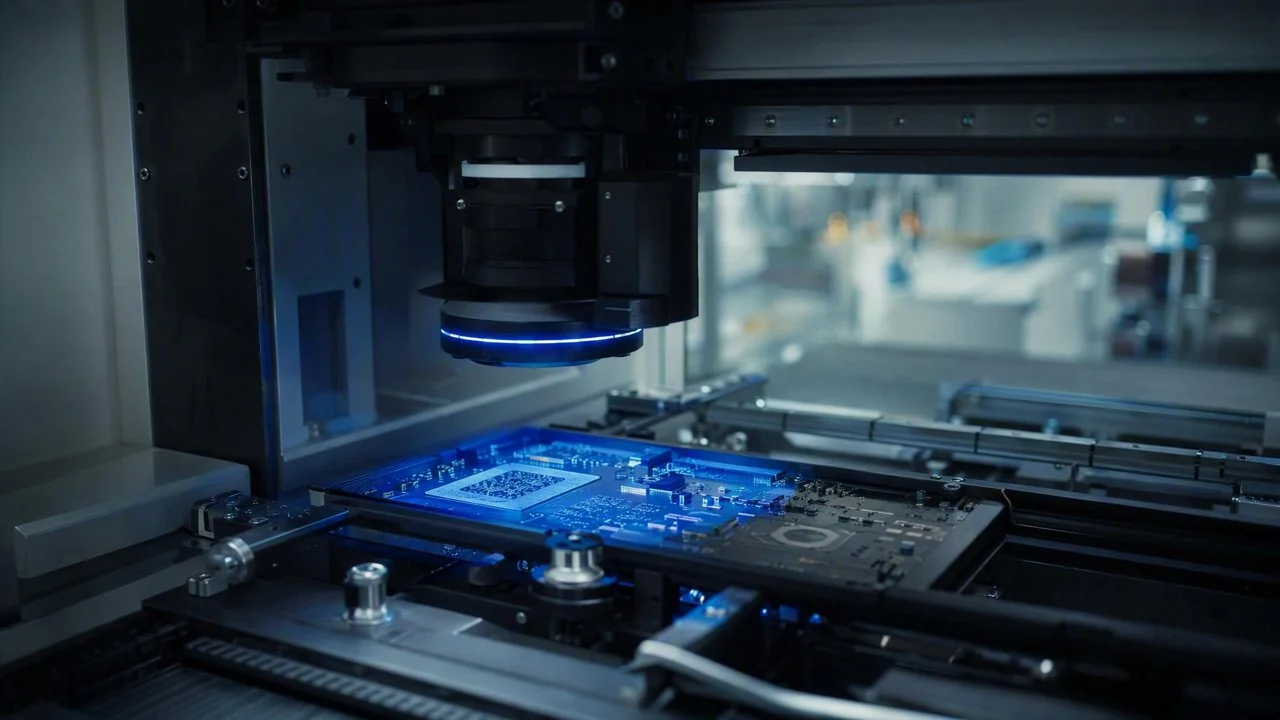
DaoAI's 3D ACI equipment, leveraging proprietary 3D cameras and 3D morphological reconstruction/point cloud technology, precisely detects hidden solder joints, coplanarity, micron-level morphology, and voids within 2D optical blind spots under BGA/QFN packages. Its 2D-3D fusion inspection capabilities reduce the labor costs associated with traditional manual visual inspection by over 70%.
In the electronics manufacturing industry, particularly on PCBA production lines, advanced packaging technologies like BGA (Ball Grid Array) and QFN (Quad Flat No-Lead) have become mainstream due to their high integration and miniaturization advantages. However, the solder joints for these package types are located beneath the component body, creating inherent 2D optical blind spots that make effective detection challenging for traditional 2D AOI equipment. For a long time, the inspection of these critical defects has heavily relied on intensive, labor-intensive manual visual inspection, which is not only inefficient but also demands extreme operator experience and concentration, directly driving up production costs and quality risks. DaoAI deeply understands this industry pain point and is committed to providing customers with more economical and efficient solutions through innovative 3D ACI technology.
Pain Points: Why This Hurdle Is Difficult to Overcome
Hidden solder joint inspection for BGA/QFN packages faces multiple challenges. First is the **extremely high labor cost**: Traditionally, manufacturers must invest a large number of skilled workers for piece-by-piece visual inspection. Each production line might require 3-5 quality inspectors working in shifts, with annual labor costs reaching hundreds of thousands of yuan. This constitutes a heavy burden for enterprises in the context of rising labor costs. Second is the **inspection efficiency bottleneck**: Manual visual inspection is slow, with single-board inspection times reaching tens of seconds or even minutes, severely slowing down the overall production line rhythm and failing to meet the demands of large-scale mass production. Furthermore, **both missed detections and false positives coexist**: Human eyes are prone to fatigue, and sensitivity to tiny defects decreases, leading to high rates of missed detections for hidden defects like BGA solder joint collapse, cold solder joints, and voids, potentially ranging from 1-3%. If these defects flow downstream, they can lead to costly rework or even product recalls. At the same time, due to subjective judgment and visual deviations, manual false positive rates are also high, adding unnecessary re-inspection steps. Finally, **data traceability and management are difficult**: Manual inspection results often lack standardized records, making it difficult to form an effective data closed loop, which hinders quality traceability and process improvement. These root problems all point to the inadequacy of traditional inspection solutions in dealing with modern high-density electronic packaging.
From a process and imaging perspective, BGA/QFN solder joints are located beneath the component body and are obscured, making it impossible for traditional 2D plane image-based AOI technology to directly obtain solder joint morphology information. Even traditional 3D inspection methods like X-Ray, while capable of penetrating internal structures, have high equipment costs, and image analysis and defect judgment still require extensive manual intervention, lacking in efficiency and automation. Moreover, micron-level changes in solder joint morphology, such as slight collapse, bridging, or voids, demand extremely high imaging resolution and algorithm recognition accuracy. In the current industry trend emphasizing AI inspection large models for improving defect detection rates and shortening development cycles, how to apply advanced AI vision technology to these 'optical blind spot' defects and effectively replace high-cost manual inspection has become an urgent problem for electronic manufacturing enterprises.
Technical Principles
The core advantage of DaoAI's 3D ACI equipment lies in its proprietary 3D camera and advanced 3D morphological reconstruction algorithms. We utilize multi-frequency phase deflectometry technology, projecting a series of high-precision structured light patterns onto the surface of the object under inspection and simultaneously capturing images from different angles with high-resolution cameras. These captured images contain micron-level height information of the object's surface. Through complex phase unwrapping algorithms and triangulation principles, precise 3D morphological point cloud data of BGA/QFN solder joints can be reconstructed. This means that even if a solder joint is obscured by the component body, as long as there are minute geometric changes on its surface, DaoAI's 3D ACI equipment can infer defect characteristics in the hidden area through its edge and side wall reflection information, combined with surrounding environmental data, using point cloud fusion and surface fitting techniques.
Unlike traditional 2D AOI, which relies on planar features like surface color and brightness, DaoAI's 3D ACI equipment directly acquires and analyzes the Z-axis height information and complete geometric contours of solder joints. For example, for BGA solder ball collapse, a 2D image might only show blurred edges, while 3D data can clearly present an abnormal reduction in solder ball height. For QFN pad voids or pores, a 2D image might be unable to detect them, but 3D morphological reconstruction can capture micron-level depressions or unevenness on the pad surface. Furthermore, DaoAI ACI OS's built-in visual foundation model can perform deep learning with 2D-3D fused data. Through APDT positive/few-shot learning (requiring only 1-20 good product images), it can quickly establish defect recognition models and utilize semantic false positive filtering technology to reduce the false positive rate to less than one-fifth of traditional rule-based AOI. This deeply integrated detection capability significantly outperforms mere 2D AOI and X-Ray solutions that require manual interpretation, achieving true automation and intelligence.
Typical Application Scenarios
- **BGA Solder Joint Collapse and Cold Solder Joint Detection**: DaoAI's 3D ACI equipment can precisely measure the height, volume, and coplanarity of BGA solder balls. Even if solder balls are located beneath the component, it can identify abnormal collapse or cold solder joints through surrounding morphology and scattered light information, combined with 3D point cloud data. The difficulty lies in the dense arrangement of solder balls and their mutual occlusion, making differentiation difficult with traditional methods.
- **QFN Pad Void and Pore Detection**: For voids or pores at the connection between the QFN package bottom pad and the PCB, which are usually located inside or at the edge of the pad, 2D images cannot directly observe them. DaoAI 3D ACI, through high-precision 3D morphological reconstruction, can detect micron-level depressions, protrusions, or unevenness on the pad surface, indirectly or directly indicating internal defects.
- **BGA/QFN Bridging and Short Circuit Risk Assessment**: In densely packaged areas, adjacent solder joints may bridge due to excessive solder or collapse. DaoAI 3D ACI equipment can accurately measure solder joint spacing and solder height, and through 3D morphological analysis, identify potential short circuit risks, with accuracy reaching micron-level.
- **Component Coplanarity and Lifted Component Detection**: The coplanarity of BGA/QFN components with the PCB directly affects soldering quality. DaoAI 3D ACI can accurately measure warping or lifting at the bottom of components, ensuring that all solder joints make full contact with the pads, avoiding open circuits or poor contact.
- **Micron-level Morphological Defect Detection**: In addition to the typical defects mentioned above, DaoAI 3D ACI can also be used to detect micron-level morphological defects such as pad surface scratches, foreign objects, and slight oxidation. These defects may be difficult to detect in 2D images due to insufficient contrast but can be clearly presented in 3D data.
Case Study
A leading Tier-1 electronics manufacturing supplier in East China produces millions of high-end PCBAs containing BGA and QFN packages monthly. Previously, their hidden solder joint inspection for BGA/QFN relied entirely on manual visual inspection, employing nearly 20 quality inspectors working three shifts. The immense labor costs and growing labor shortage issues prompted them to urgently seek automated solutions. Before implementing DaoAI's 3D ACI equipment, their average single-board inspection time for manual visual inspection was 45 seconds, limiting production line rhythm. Additionally, due to eye fatigue, the missed detection rate for BGA cold solder joints averaged around 0.8%, resulting in significant rework and scrap losses each month. After a thorough analysis of the customer's needs, the DaoAI team deployed the 3D ACI equipment. In the initial phase, leveraging the APDT few-shot learning capability of the DaoAI ACI OS, we completed the training of defect detection models for BGA cold solder joints, collapse, QFN voids, and other defects in just 20 minutes, using only 15 good product images. After two weeks of parallel testing and optimization, DaoAI's 3D ACI equipment successfully achieved fully automated inspection.
DaoAI's 3D ACI equipment successfully reduced the customer's hidden solder joint manual re-inspection rate by 83%, significantly optimizing production line labor costs.
DaoAI Solutions and Products
The core solution provided by DaoAI to this leading manufacturer is the 3D ACI equipment, based on its proprietary 3D camera and 3D morphological reconstruction technology. This equipment, through high-precision structured light projection and multi-view image acquisition, reconstructs complete 3D point cloud data of BGA/QFN solder joints, thereby achieving precise detection of hidden solder joints, coplanarity, voids, and other defects in 2D optical blind spots. Combined with the DaoAI ACI OS, we achieved 2D-3D fusion inspection, utilizing the visual foundation model's feature recognition capabilities to complete 0-code automatic programming in 5 minutes for a single good product. Through APDT positive/few-shot learning, even for new package types, deployment can be achieved quickly with 1-20 good product samples. DaoAI's solution also supports 100% local private deployment (SDK/API/Docker), ensuring customer data remains on-site and meeting their strict data security and compliance requirements. Furthermore, DaoAI World Model, as a unified foundation, enables cross-scenario generalization and continuous learning from production line feedback, further enhancing the robustness and adaptability of detection models. Through the combination of these products and capabilities, DaoAI provides a comprehensive, efficient, and economical automated inspection solution.
By deploying DaoAI's 3D ACI equipment, the manufacturer achieved significant quantified results. First, **manual visual inspection demand was greatly reduced**: The original 20-person quality inspection team now only requires 3-4 people for equipment monitoring and a small amount of anomaly review, reducing labor costs by over 70% and saving nearly one million yuan in annual labor costs. Second, **inspection efficiency was significantly improved**: Single-board inspection time was reduced from 45 seconds to 8 seconds, increasing the production line rhythm by 460%, greatly boosting overall capacity. Third, **defect missed detection rates were significantly reduced**: The missed detection rate for BGA cold solder joints dropped from 0.8% to <0.1%, fundamentally guaranteeing product quality and effectively avoiding costly backend rework and customer complaints. Finally, **data traceability was enhanced**: All inspection data is recorded and analyzed by the system in real-time, providing valuable data support for quality traceability and process optimization. These achievements fully demonstrate the immense value of DaoAI's 3D ACI equipment in replacing manual visual inspection and optimizing labor costs.
FAQ
How does DaoAI's 3D ACI equipment solve the blind spot problem in BGA/QFN hidden solder joint inspection?
DaoAI's 3D ACI equipment utilizes proprietary high-precision 3D cameras and multi-frequency phase deflectometry to reconstruct complete 3D morphological point cloud data of solder joints. Even if solder joints are obscured by the component body, it can accurately identify defects such as collapse, cold solder joints, and voids through micron-level morphological changes on their edges, side walls, and scattered light information, combined with advanced 2D-3D fusion AI algorithms, effectively overcoming traditional 2D optical blind spots.
What are the advantages of DaoAI's 3D ACI for BGA/QFN solder joint inspection compared to traditional X-Ray inspection?
Compared to X-Ray, DaoAI's 3D ACI equipment offers significant advantages in cost, efficiency, and automation. X-Ray equipment is typically expensive, and image analysis and defect judgment still require extensive manual intervention. Our 3D ACI equipment has lower acquisition costs and achieves fully automated judgment through AI algorithms, greatly increasing inspection speed and reducing reliance on operator expertise. It also supports inline full inspection, making it more suitable for high-throughput production lines.
What is the budget for deploying DaoAI's 3D ACI equipment, and what factors influence the price?
The deployment cost of DaoAI's 3D ACI equipment is influenced by various factors, including production line speed, required inspection accuracy, product dimensions to be inspected, necessary detection function modules (e.g., whether 2D-3D fusion or specific defect type recognition is needed), and deployment method (e.g., integration into an existing production line or standalone deployment). We offer flexible configuration options, and specific quotations are customized based on the customer's actual needs and technical solution. We recommend contacting our sales team to schedule a technical consultation, and we will provide you with a detailed solution and accurate quotation.
Full solution for this scenario: Electronics / PCBA industry solutions
This article was generated by AI. Customer cases are simulated scenarios based on real product capabilities and figures are illustrative; see product pages for official benchmarks.