
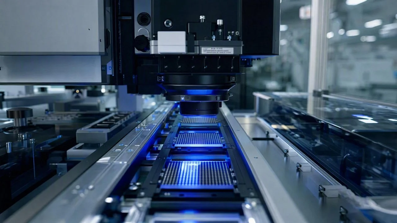
In semiconductor packaging, DaoAI's 3D ACI equipment, leveraging proprietary 3D cameras and 3D morphology reconstruction/point cloud technology, effectively detects hidden solder joints, coplanarity issues, micron-level morphology, and pores – defects often missed by 2D optics. Its 2D-3D fusion capability reduces micro bump defect inspection time per chip by 35%, significantly boosting production throughput and 100% inspection capacity.
In semiconductor packaging, DaoAI's 3D ACI equipment, utilizing proprietary 3D cameras and 3D morphology reconstruction/point cloud technology, effectively detects hidden solder joints, coplanarity issues, micron-level morphology, and pores – defects often missed by 2D optics. Its 2D-3D fusion capability reduces micro bump defect inspection time per chip by 35%, significantly boosting production throughput and 100% inspection capacity. The semiconductor industry's relentless pursuit of quality means that even the slightest defect can lead to chip failure. Especially in the micro bump process for Flip Chip packaging, these bumps are critical connections between the chip and substrate, directly impacting electrical performance and reliability. As chip sizes shrink and integration increases, micro bump pitches have reached micron levels, with vast numbers arranged densely, posing severe challenges to inspection technologies. Traditional sampling methods can no longer meet high reliability requirements, while 100% inspection faces immense pressure on production throughput.
Pain Points: Why This Hurdle Is So Difficult to Overcome
In micro bump inspection, traditional solutions face multiple challenges. First, there's a **conflict between production throughput and 100% inspection capacity**: A leading semiconductor packaging manufacturer, whose production line processes hundreds of chips per minute, found that traditional 2D AOI could detect some defects but struggled with 3D morphological defects of micro bumps (e.g., height, coplanarity anomalies). This necessitated manual re-inspection, extending single-chip inspection time to several seconds, far below the required production beat, making 100% inspection a bottleneck. Second, the **escape rate for micron-level defects remained high**: Defects like missing, bridged, collapsed, or uneven micro bumps might not be obvious in 2D images, especially when pads and bumps have similar colors. Traditional 2D optical inspection's escape rate was as high as 0.8% or more. This directly led to soaring rework costs in subsequent processes and even customer complaints. Third, **re-inspection burden due to false positives**: Traditional rule-based 2D AOI is susceptible to interference from lighting, surface reflections, and background textures, generating numerous false positives. This resulted in manual re-inspection accounting for over 30% of labor hours, severely draining human resources. Finally, **difficulty in identifying complex defects**: Micro bumps are 3D structures, and their height, volume, and coplanarity are critical quality indicators. Traditional 2D imaging cannot provide this information, making it difficult to effectively identify 3D defects such as the “Pillow Effect” or slight collapses.
The root cause of these problems lies in the complexity of semiconductor packaging processes and the physical properties of micro bumps themselves. Micro bump diameters are typically between 20-100 microns, with heights of only tens of microns, arranged in dense arrays with extremely small pitches. Traditional 2D cameras can only capture planar information, completely failing to provide 3D morphological features like height, volume, and coplanarity. Moreover, the complex reflective properties of micro bump materials (e.g., SnAgCu alloy) often create highlights or shadows in 2D images, interfering with defect judgment. The current trend of digital twin technology precisely requires accurate, real-time 3D data as its foundation. If high-precision 3D morphological data cannot be acquired in real-time at the front end of the production line, it becomes challenging to build accurate digital twin models, let alone manage and optimize the entire lifecycle of industrial production lines, including predictive maintenance and process parameter optimization. All optimization efforts would lack data support.
Technical Principles
The core of DaoAI's 3D ACI equipment lies in its **proprietary high-precision 3D camera and advanced 3D morphology reconstruction algorithms**. The equipment employs multi-frequency structured light projection technology combined with the phase-shifting method. It projects a series of specific grating patterns onto the surface of the object under test and captures the deformed images with a high-resolution industrial camera. These image sequences are processed by DaoAI's unique 3D morphology reconstruction algorithms, which precisely calculate the phase information for each pixel, then derive its depth value in the Z-axis direction, ultimately generating high-precision point cloud data. This point cloud data contains complete 3D morphological information of the micro bump surface, with micron-level accuracy. Unlike traditional 2D AOI, which relies solely on grayscale or color information, DaoAI's 3D ACI can directly acquire critical 3D parameters such as bump height, volume, coplanarity, and tilt angle. For example, for missing or collapsed micro bumps, a 2D image might only show a change in brightness, easily confused with shadows; however, 3D data clearly reveals the height collapse or absence in that area, preventing misjudgment. Furthermore, DaoAI's 2D-3D fusion technology is not a simple image overlay; it deeply integrates 2D image texture and color information with 3D point cloud geometric information, allowing AI models to analyze both data types simultaneously for more comprehensive and robust defect identification.
Compared to traditional rule-based 2D AOI, DaoAI's 3D ACI has achieved a qualitative leap in detection capabilities. Traditional 2D AOI struggles to differentiate missing defects when pad and bump colors are similar, and cannot accurately determine bump height and coplanarity. In contrast, DaoAI's 3D ACI, with its 3D data, can directly measure these parameters, controlling micro bump height detection accuracy within ±2 microns and precisely calculating coplanarity. Compared to manual visual inspection, DaoAI 3D ACI not only significantly improves detection speed and consistency, avoiding human eye fatigue and subjective judgments that lead to escapes and false positives, but also demonstrates significant advantages in complex defect identification. For instance, for micro bump bridging, a 2D image might be blurry due to angle or lighting issues, but 3D data can clearly show the physical connection between two bumps, enabling high-precision judgment. DaoAI's ACI OS, combined with APDT few-shot learning capabilities, requires only 1-20 good samples to quickly complete model training, greatly shortening changeover time and supporting 5-minute 0-code automatic programming, further enhancing production line efficiency.
Typical Application Scenarios
- **Missing and Bridged Micro Bump Detection**: DaoAI's 3D ACI precisely reconstructs 3D morphology to clearly identify whether micro bumps are completely missing or bridged with other bumps. The challenge lies in the small size and dense spacing of micro bumps, where 2D images are prone to reflection interference, while 3D data provides accurate physical connection information.
- **Micro Bump Height and Coplanarity Detection**: The equipment can accurately measure the height of each micro bump and calculate the coplanarity of the entire array. This is crucial for controlling the contact resistance and stress distribution between the chip and substrate. The difficulty lies in micron-level accuracy requirements and rapid measurement of large-scale arrays.
- **Micro Bump Collapse and Shape Anomalies**: For micro bumps experiencing collapse, deformation, or insufficient sphericity due to improper welding processes, DaoAI 3D ACI can precisely distinguish these shape anomalies from their 3D contours. Traditional 2D images struggle to capture these subtle 3D deformations.
- **Pad Contamination and Foreign Object Detection**: Before and after micro bump formation, inspect the pad surface for foreign objects, flux residue, or contamination. While some can be detected by 2D inspection, DaoAI's 2D-3D fusion technology provides more comprehensive surface information, especially for transparent or low-contrast foreign objects.
- **Pore and Void Detection**: Pores may exist inside or at the base of micro bumps, affecting conductivity and reliability. DaoAI's 3D ACI, combined with its morphology reconstruction capabilities, can identify surface pore features, providing preliminary information for further X-ray inspection and improving overall detection efficiency.
Case Study
A leading domestic integrated circuit packaging and testing manufacturer faced long-standing challenges in micro bump inspection. Their production line demanded extremely high throughput, and traditional 2D AOI inspection equipment could not meet the capacity requirements for 100% inspection, leading to some high-value chips being subjected to sampling inspection, posing potential quality risks. Simultaneously, due to the minute size and reflective nature of micro bumps, traditional 2D AOI's false positive rate exceeded 15%, and the escape rate hovered around 0.7%, with extensive manual re-inspection consuming valuable production time and severely hindering overall efficiency. The manufacturer introduced DaoAI's 3D ACI equipment for a pilot run. During the initial deployment, DaoAI's engineering team worked closely with the client, utilizing the APDT few-shot self-training feature. With only 15 good samples, they rapidly trained models for various defects such as missing, bridged, and height-anomalous micro bumps within a few hours. Upon commissioning, the equipment immediately demonstrated outstanding performance. DaoAI's 3D ACI reduced single-chip inspection time from 3.2 seconds to 2.1 seconds, achieving a significant improvement in production throughput and successfully meeting the capacity requirements for 100% inspection. Concurrently, thanks to precise 3D morphological data and advanced AI algorithms, the false positive rate decreased by 85%, and the escape rate was reduced to <0.2%, substantially decreasing the workload of manual re-inspection and saving nearly a million RMB in labor costs annually. The manufacturer's production manager stated that DaoAI's 3D ACI not only improved product quality but also optimized the entire production process, providing a solid foundation for subsequent smart manufacturing upgrades.
"DaoAI's 3D ACI equipment not only improved our inspection accuracy, but more importantly, it allowed us to achieve 100% micro bump inspection for the first time, without sacrificing production throughput. This has completely changed our quality control model."
DaoAI Solutions and Products
DaoAI's core offering for semiconductor micro bump inspection is the **DaoAI 3D ACI equipment**. This equipment integrates DaoAI's proprietary high-precision 3D camera, a high-performance edge computing platform, and the DaoAI ACI OS. For model building, we employ the APDT positive/few-shot learning mechanism, where customers only need to provide a small number of good samples (1-20 images) to complete 0-code automatic programming in 5 minutes, quickly generating highly robust defect detection models. This greatly simplifies model deployment and maintenance. For multi-variety, small-batch production modes, this rapid changeover capability is crucial. The 2D-3D fusion detection capability of DaoAI's 3D ACI ensures comprehensive coverage of micro bumps from planar to three-dimensional, filling the blind spots of traditional 2D optical inspection. Furthermore, the DaoAI ACI OS features semantic false positive filtering, which can effectively identify and filter out non-defect interferences (e.g., textures, light spots), further reducing the false positive rate. For deployment, DaoAI provides various flexible integration methods such as SDK/API/Docker and supports 100% local private deployment, ensuring customer data security remains on-site, meeting the stringent requirements of the semiconductor industry for data privacy and security. Combined with the unified foundation of the DaoAI World global model, the equipment can continuously learn from production line feedback, achieving self-optimization and cross-scenario generalization of models.
By deploying DaoAI's 3D ACI equipment, customers realize significant business value. First, **production throughput is substantially increased**: inspection efficiency improved by 35%, leading to an increase in single-line capacity by over 20%, effectively alleviating the capacity pressure of 100% inspection. Second, **product quality and reliability are significantly enhanced**: the micro bump escape rate is reduced to <0.2%, effectively avoiding potential failure risks and improving the overall chip yield. Third, **operating costs are significantly reduced**: the false positive rate decreased by 85%, substantially reducing the need for manual re-inspection and freeing up a large amount of human resources, directly lowering production costs. Finally, **data assets and process optimization capabilities are strengthened**: high-precision 3D inspection data provides a reliable basis for subsequent digital twin construction and process parameter optimization, helping customers achieve smarter and more efficient semiconductor manufacturing.
FAQ
What is the fundamental difference between DaoAI's 3D ACI equipment and traditional 2D AOI?
The fundamental difference of DaoAI's 3D ACI lies in its proprietary 3D camera and 3D morphology reconstruction capabilities. Traditional 2D AOI can only acquire planar images, unable to detect 3D information such as height, coplanarity, and volume. In contrast, 3D ACI can precisely reconstruct the complete 3D morphology of the object under test, thus detecting defects in 2D optical blind spots, such as micro bump height collapse, tilt, and coplanarity anomalies, while achieving 2D-3D fusion inspection, greatly enhancing the comprehensiveness and accuracy of detection.
What is the approximate budget required to deploy DaoAI's 3D ACI equipment?
The budget for DaoAI's 3D ACI equipment depends on various factors, including specific configurations, complexity of the inspection objects, production line integration requirements, and whether customized functionalities are needed. We offer flexible solutions and support 100% local private deployment. We recommend scheduling a consultation with our experts for detailed discussions, and we will provide a customized quotation and ROI analysis based on your specific requirements.
How does DaoAI's 3D ACI ensure inspection efficiency and 100% full inspection capacity on high-speed production lines?
DaoAI's 3D ACI ensures extremely high efficiency in image acquisition and data processing through its high-speed proprietary 3D camera combined with optimized 3D morphology reconstruction algorithms and a high-performance edge computing platform. Concurrently, the DaoAI ACI OS utilizes lightweight, highly efficient AI models, combined with APDT few-shot learning, to achieve rapid model training and precise defect identification. This combination of technologies enables the equipment to perform high-precision, 100% full inspection without impacting production throughput, significantly boosting overall capacity.
Full solution for this scenario: the full inspection solution for Semiconductor / chips
This article was generated by AI. Customer cases are simulated scenarios based on real product capabilities and figures are illustrative; see product pages for official benchmarks.