
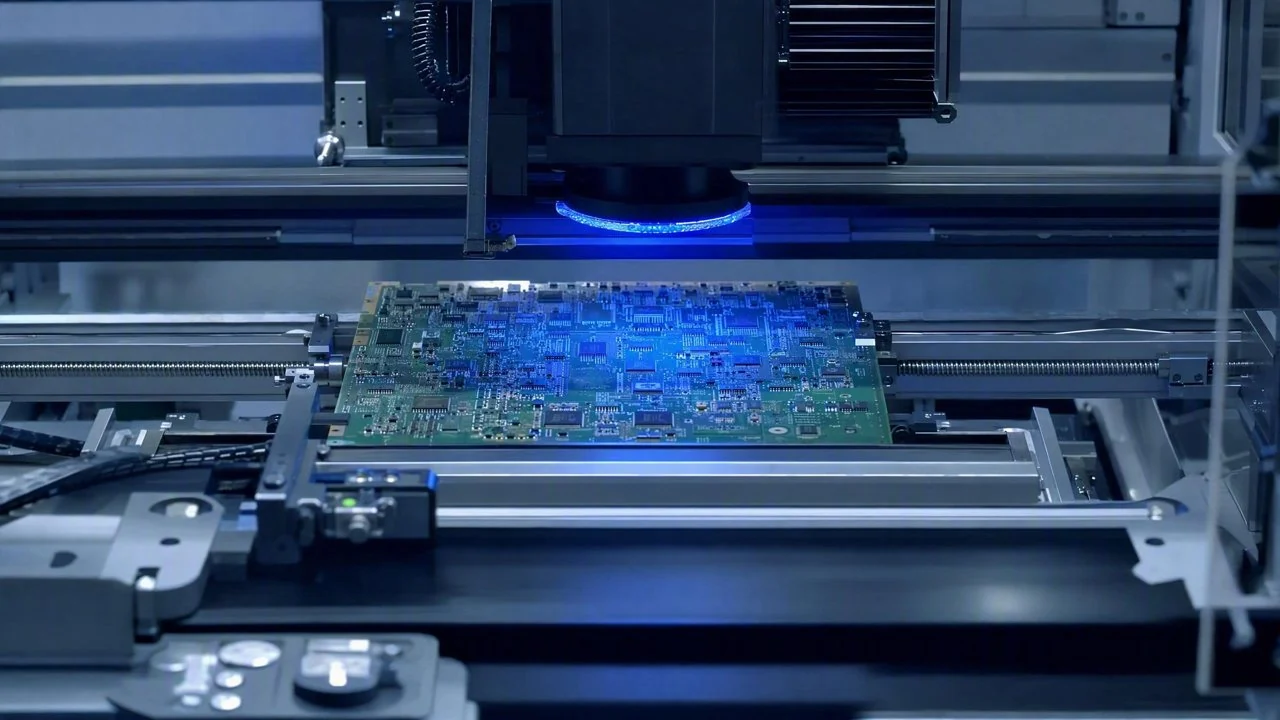
DaoAI 3D ACI equipment (proprietary 3D camera + 3D morphology reconstruction/point cloud, detecting hidden solder joints/coplanarity/micron-level morphology/voids and other 2D optical blind spot defects, 2D-3D fusion), by precisely quantifying 3D solder joint morphology and applying AI intelligent discrimination, reduces BGA void detection false positives from an industry average of 10–15% to <2%, significantly optimizing quality control and production efficiency for BGA packages in electronics / PCBA manufacturing. In the rapidly evolving field of electronics manufacturing, the quality of PCBA (Printed Circuit Board Assembly) is the cornerstone of product performance and reliability. Especially in BGA (Ball Grid Array) packages, solder joint voids are common defects that severely impact electrical conductivity, heat dissipation, and mechanical strength. A leading supplier specializing in high-end communication equipment PCBA manufacturing, whose products demand extremely high BGA solder joint quality, faced severe challenges with traditional inspection methods.
Pain Points: Why This Hurdle Is Difficult to Overcome
This leading supplier, in the BGA void detection process, traditionally relied on X-ray equipment for initial screening, supplemented by extensive manual reinspection. However, this approach presented numerous pain points: Firstly, the 2D projection nature of traditional X-ray images made it difficult to precisely determine the boundaries, depth, and shape of voids, leading to a false positive rate as high as 10–15%. Secondly, the high false positive rate directly resulted in a massive workload for manual reinspection, requiring 3-5 experienced operators per shift for visual verification, consuming significant labor costs and time. Thirdly, the inefficiency of the reinspection process severely slowed down the overall production line takt time, affecting capacity. Finally, due to the limitations of X-ray equipment, some deep or irregularly shaped voids still posed a risk of undetected defects, which, if passed to downstream processes, would lead to product rework or even scrap, incurring huge economic losses and brand reputation risks.
The difficulty in detecting BGA voids lies in their physical characteristics and imaging principles. In PCBA manufacturing, as solder joint sizes miniaturize and packaging density increases, voids can appear anywhere within the solder ball, varying in morphology from tiny bubbles to irregular cavities. Traditional X-ray images are transmission images and do not provide depth information, making it difficult to distinguish between true defects and imaging artifacts (such as pad edge effects, layer interference). Furthermore, the increasing adoption of ultrasonic welding technology in precision assembly, while improving production efficiency and product quality, places higher demands on the internal structure of solder joints, particularly the formation and detection of micro-voids. Traditional 2D X-ray struggles to effectively differentiate micron-level voids that may arise after ultrasonic welding from normal solder joint structures, further exacerbating the challenges of false positives and missed detections.
Technical Principles
The core advantage of DaoAI 3D ACI equipment lies in its proprietary 3D camera and advanced 3D morphology reconstruction technology. Unlike traditional X-ray, which only provides 2D projection information, DaoAI 3D ACI utilizes multi-angle structured light projection and a high-resolution camera array to precisely reconstruct the complete 3D morphology of BGA solder joints by computing 3D point cloud data. This process allows for the acquisition of micron-level geometric parameters of solder joints, such as height, volume, and coplanarity, enabling precise quantification of defects both inside and on the surface of the solder joint. For BGA voids, the system no longer relies solely on 2D grayscale differences but identifies them by analyzing 'abnormal depressions' or 'internal voids' features present in the 3D point cloud data. For example, the system can accurately measure the depth, diameter, and volume of voids, and combine this with their spatial location in 3D for more accurate judgments.
At the algorithmic level, DaoAI 3D ACI equipment integrates the strengths of deep learning and traditional image processing. We employ APDT positive sample/few-shot learning technology, requiring only 1–20 good sample images to quickly train models, significantly reducing changeover time. Based on 3D point cloud data, the AI model can learn and recognize 3D features of various complex BGA voids, including shape, size, location, and depth, effectively distinguishing true defects from non-defect features. Compared to traditional rule-based AOI, which relies on engineers manually setting thresholds and rules, DaoAI's AI model boasts stronger generalization capabilities and robustness, adapting to minor process fluctuations across different batches and materials, thereby reducing the false positive rate by over 85%. Concurrently, the 2D-3D fusion detection mechanism compensates for blind spots in single-dimension detection, ensuring comprehensive coverage of 2D optical blind spot defects such as hidden solder joints, coplanarity, micron-level morphology, and voids. This allows DaoAI 3D ACI to not only control the false positive rate for BGA void detection to <2% but also maintain a detection rate of over 99.5%.
Typical Application Scenarios
- **BGA Solder Joint Void Detection:** DaoAI 3D ACI precisely identifies bubbles, cavities, and other void defects inside and on the surface of solder balls through 3D morphology reconstruction, quantifying their volume, depth, and position, avoiding misjudgments from traditional X-ray's 2D projection. The challenge lies in the diverse morphology of voids and potential occlusion by other structures.
- **Solder Joint Coplanarity and Bridging Detection:** The system accurately measures the height consistency (coplanarity) of BGA solder balls, identifying risks of open circuits or short circuits due to height differences. For bridging defects between adjacent solder balls, 3D spatial analysis effectively distinguishes open circuits from short circuits, avoiding issues with traditional 2D AOI being susceptible to shadows.
- **Lead Deformation and Missing Lead Detection:** For leads of packages like QFN/QFP, DaoAI 3D ACI can detect defects such as bent, lifted, or missing leads, ensuring compliance with design specifications by measuring their 3D position and shape. The difficulty lies in the tiny size and dense arrangement of leads.
- **Solder Volume and Solder Paste Print Quality Inspection:** In the Solder Paste Inspection (SPI) process, the equipment can accurately measure solder paste thickness, volume, area, and shape, identifying defects like print offset, bridging, or slumping, providing quality assurance for subsequent reflow soldering. The challenge lies in the rheology of solder paste and minor fluctuations during printing.
- **Component Placement Offset and Polarity Detection:** The system can highly accurately detect placement position and angle offsets, as well as polarity reversal defects for various SMT components, ensuring correct installation. Through 3D data, it can more accurately determine the alignment of components with pads, reducing misjudgments.
Case Study
A tier-1 PCBA supplier serving a global telecommunications giant, whose BGA-packaged product yield directly impacts the performance of downstream communication equipment. Before integrating DaoAI 3D ACI equipment, this supplier's BGA void detection primarily relied on a high-resolution X-ray machine for initial screening, followed by manual reinspection by a team of 5 people. Due to the inherent limitations of X-ray images, the false positive rate remained stubbornly high, averaging 12%. This meant thousands of 'suspected defects' had to be manually verified daily, leading to an enormous workload for the reinspection team and frequent missed detections due to fatigue. Production line takt time was consequently constrained, unable to meet growing order demands. To address this bottleneck, the supplier chose to deploy DaoAI 3D ACI equipment for online full inspection.
After the deployment of DaoAI 3D ACI equipment, this client's BGA void detection false positive rate decreased by over 85%, manual reinspection personnel were reduced from 5 to 1, and overall production line efficiency improved by 15%.
The DaoAI team first conducted two weeks of on-site data collection and model training at the client's production line. Utilizing the APDT positive sample learning capability of the DaoAI ACI OS, a void detection model tailored to the client's product characteristics was quickly built and optimized using just 15 good sample PCB board BGA images. After deployment, its proprietary 3D camera combined with 3D morphology reconstruction technology could precisely identify micron-level voids within BGA solder balls, providing quantified data on depth and volume. Compared to traditional X-ray, DaoAI 3D ACI equipment effectively differentiated pad edge artifacts from true voids, reducing the false positive rate from 12% to <1.8%, a significant reduction of over 85%. This drastically reduced the manual reinspection workload, with personnel decreasing from 5 to just 1 for spot checks, greatly alleviating the labor burden and improving overall production line efficiency by 15%. The client highly praised DaoAI 3D ACI equipment's performance in reducing false positives and easing reinspection burden.
DaoAI Solutions and Products
The core solution provided by DaoAI is based on the DaoAI 3D ACI equipment, which integrates our proprietary high-precision 3D camera and powerful 3D morphology reconstruction algorithms, specifically designed to solve complex defect detection challenges like BGA voids in the PCBA industry. This equipment can perform micron-level 3D morphology measurements on solder joints, acquiring critical data such as depth, volume, and coplanarity, thereby enabling precise identification of defects in 2D optical blind spots. In terms of deployment, DaoAI 3D ACI supports 100% on-premise private deployment, ensuring customer data remains in-house and meeting strict data security and compliance requirements. Through the DaoAI ACI OS, customers can utilize its zero-code automatic programming and APDT positive sample/few-shot learning features to quickly achieve new product changeovers, typically completing model training and deployment within 5 minutes, significantly enhancing production line flexibility and efficiency.
Furthermore, DaoAI World World Model, as a unified foundation, endows the 3D ACI with stronger semantic understanding and cross-scenario generalization capabilities, enabling it to continuously learn from production line feedback, constantly optimizing detection accuracy and robustness. Coupled with the semantic false positive filtering function of the DaoAI ACI OS, it further enhances the accuracy of defect judgment, reducing the false positive rate of BGA void detection to an extremely low level. Through the combination of these advanced technologies, DaoAI 3D ACI equipment not only significantly reduces customer false positive rates and manual reinspection costs but also improves product quality and overall production line efficiency, delivering tangible business value to customers.
FAQ
What is the fundamental difference between DaoAI 3D ACI equipment and traditional X-ray for BGA void detection?
DaoAI 3D ACI equipment utilizes proprietary 3D cameras and 3D morphology reconstruction technology to directly acquire 3D point cloud data of solder joints, enabling precise quantification of void depth, volume, and shape. Traditional X-ray, however, only provides 2D transmission images, making it difficult to distinguish true voids from imaging artifacts, leading to high false positive rates. Our solution offers more comprehensive 3D information, combined with AI intelligent discrimination, significantly improving detection accuracy and reducing false positives.
How long does it typically take to deploy DaoAI 3D ACI equipment, and will it affect existing production line takt time?
DaoAI 3D ACI equipment can typically be deployed and debugged within a few weeks. We support 100% on-premise private deployment, ensuring customer data remains in-house. Initial model training, based on APDT positive sample learning, can be quickly completed with just 1–20 good samples. During operation, the equipment's high-speed detection capabilities are highly synchronized with the production line takt time, and can even improve overall efficiency. It will not negatively impact existing production lines; instead, it enhances overall throughput by reducing manual reinspection.
What are the main cost components of DaoAI 3D ACI equipment? How is the return on investment (ROI) period evaluated?
The primary costs for DaoAI 3D ACI equipment include hardware, AI software system licenses, deployment services, and ongoing maintenance support. Specific pricing varies based on client production line scale, inspection requirements, and customization needs. When evaluating the ROI period, one must consider the savings in reinspection labor costs due to reduced false positives, the prevention of rework and scrap losses from lower missed detection rates, and the increased production capacity resulting from improved line efficiency. We recommend scheduling an expert consultation to receive a customized cost analysis and ROI projection report.
This article was generated by AI. Customer cases are simulated scenarios based on real product capabilities and figures are illustrative; see product pages for official benchmarks.