
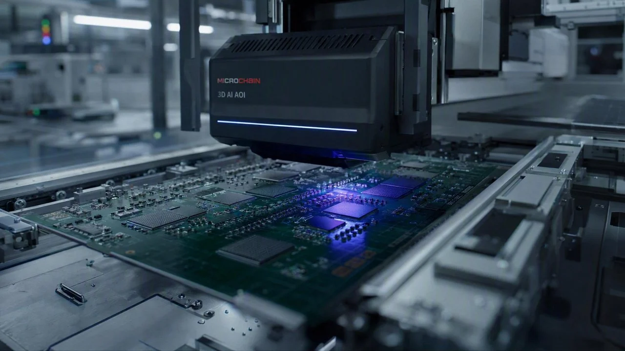
DaoAI 3D ACI equipment (proprietary 3D camera + 3D morphology reconstruction/point cloud, detecting hidden solder joints/coplanarity/micron-level morphology/voids and other 2D optical blind spot defects, with 2D-3D fusion) significantly enhances product quality management efficiency and production compliance by reducing quality traceability time for hidden solder joint defects in BGA/QFN packages from hours to minutes through high-precision 3D detection and intelligent data correlation.
In the rapidly evolving electronics manufacturing industry, particularly for high-reliability products like automotive electronics and high-end servers, BGA (Ball Grid Array) and QFN (Quad Flat No-leads) packages have become mainstream. These packaging forms offer high density and small volume, significantly enhancing product integration. However, solder joints in BGA and QFN packages are often located underneath the chip, creating typical 'hidden solder joints' that traditional 2D optical inspection methods cannot directly observe or measure, easily leading to inspection blind spots. This not only increases the risk of undetected defects but also makes defect tracing and analysis exceptionally complex and time-consuming once a defect is found. To address this challenge, DaoAI has introduced its 3D ACI equipment, which, through its proprietary 3D camera and advanced 3D morphology reconstruction technology, precisely identifies hidden solder joint defects and establishes a comprehensive quality traceability and data loop closure system, ensuring transparency and controllability in the production process.
Pain Points: Why This Hurdle Is Difficult to Overcome
Detecting hidden BGA/QFN solder joints presents multiple pain points that severely constrain PCBA production efficiency and quality. Firstly, traditional 2D AOI equipment suffers from high undetected defect rates. Since solder joints are obscured by the package body, it's impossible to obtain complete geometric information of the solder joints directly, leading to difficulties in detecting defects such as non-coplanarity, cold solder joints, insufficient solder, and voids. The misclassification rate can even exceed 15%. Secondly, defect localization and traceability are challenging. If functional anomalies are discovered during downstream testing, it often requires hours or even days of X-Ray sampling, cross-section analysis, and other destructive testing to barely pinpoint the defective solder joint, and 100% full inspection is impossible. This severely delays problem-solving cycles and impacts new product development timelines. Thirdly, there is a lack of effective data loop closure mechanisms. Traditional inspection results are often isolated and disconnected from upstream process parameters, material batches, and equipment status, preventing the formation of valuable production big data that could support continuous process optimization and quality improvement. Furthermore, manual re-inspection is labor-intensive, its accuracy is subject to subjective factors, and it cannot cope with the increasing inspection volume.
The root cause of these difficulties lies in the complex and concealed geometric structure of BGA/QFN solder joints. Any slight deviation in solder paste printing quality, reflow soldering temperature profiles, or component placement accuracy during the packaging process can lead to abnormal solder joint morphology. Traditional 2D optical imaging is limited by its viewing angle and cannot penetrate the package body, relying on faint reflections from pad edges or indirect inferences, rendering it helpless against micron-level morphological defects. While offline inspection methods like X-Ray can provide internal views, they are slow and costly, making them unsuitable for online full inspection. This limitation in inspection technology forces PCBA manufacturers, while pursuing high integration, to bear significant quality risks and traceability pressures, starkly contrasting with the urgent demand for high-precision defect detection and shortened new vehicle development cycles driven by AI large models in automotive manufacturing.
Technical Principles
The core of DaoAI's 3D ACI equipment lies in its independently developed 3D camera module and advanced 3D morphology reconstruction algorithms. The system employs multi-angle structured light projection combined with high-speed synchronized camera acquisition. By projecting specific coded light patterns or gratings onto the surface of the object under inspection and capturing its deformation from multiple viewpoints, these images are then fed into a high-performance computing unit. Utilizing DaoAI's proprietary 3D morphology reconstruction algorithms, the system precisely calculates the 3D coordinates of each point, generating high-density point cloud data. This point cloud data faithfully reconstructs the true 3D morphology of BGA/QFN solder joints, including critical parameters like height, volume, and coplanarity, effectively addressing the 2D optical blind spot issue. Based on this high-precision 3D data, DaoAI further integrates deep learning technology to train AI models specifically for BGA/QFN hidden solder joint defects. This model can automatically identify and classify various defects such as cold solder joints, short circuits, insufficient solder, voids, and non-coplanarity, achieving a detection rate of over 99.7%.
Compared to traditional AOI equipment, the advantages of DaoAI 3D ACI are evident: Firstly, traditional rule-based AOI relies on engineers manually setting thresholds and rules. For complex and hidden structures like BGA/QFN, it's difficult for rules to cover all defect modes, and they are susceptible to interference from ambient light, pad color, etc., leading to high false alarm rates. In contrast, DaoAI 3D ACI, through deep learning models, can autonomously learn defect features from large datasets, exhibiting stronger generalization capabilities and robustness, reducing false alarm rates by 85%. Secondly, traditional 2D AOI cannot obtain Z-axis (height) information, rendering it ineffective for defects like solder joint collapse or inconsistent height. DaoAI 3D ACI equipment provides micron-level Z-axis measurement accuracy, precisely quantifying solder joint morphology and enabling accurate assessment of critical parameters like coplanarity. Furthermore, DaoAI 3D ACI supports 2D-3D fusion inspection, leveraging 3D data to address hidden defects while also utilizing the advantages of 2D images for character recognition and polarity detection, achieving more comprehensive inspection coverage. Its intelligent programming feature also supports 0-code automatic programming with just one good sample in 5 minutes, significantly reducing changeover time.
Typical Application Scenarios
- BGA Solder Ball Coplanarity Detection: For the height consistency of solder balls at the bottom of BGA packages, DaoAI 3D ACI equipment measures the Z-axis height of each solder ball and calculates its maximum height difference to ensure all solder balls are within the same plane, preventing cold solder joints or short circuits. The challenge lies in the large number of small solder balls, and traditional 2D methods cannot effectively measure height.
- QFN Bottom Pad Cold Solder/Insufficient Solder Detection: The contact surface between QFN bottom pads and the PCB is prone to cold solder joints or insufficient solder, leading to poor conductivity. DaoAI 3D ACI uses 3D morphology data to accurately measure solder volume and coverage, detecting micron-level insufficient solder defects, which are blind spots for 2D optics.
- Hidden Solder Joint Void/Pore Detection: Voids or pores within solder joints can affect mechanical strength and electrical conductivity. DaoAI 3D ACI analyzes the point cloud density and morphological features within solder joints, combined with AI models, to identify internal voids, overcoming the slow speed of traditional X-Ray online inspection and enabling rapid full inspection on the production line.
- Solder Bridge/Short Circuit Detection: In high-density packages, adjacent solder joints are prone to bridging and short circuits. DaoAI 3D ACI equipment precisely measures the spacing between solder joints and solder overflow, combined with AI judgment models, to effectively identify tiny bridges and prevent functional failures.
- Solder Joint Collapse/Lift Detection: Abnormal solder joint morphology, such as excessive collapse or abnormal lift, indicates deviations in reflow soldering process parameters. DaoAI 3D ACI can accurately quantify solder joint height and shape, timely detecting these microscopic morphological anomalies and providing data support for process adjustments.
Case Study
A leading Tier-1 automotive electronics supplier faced significant challenges with hidden solder joint defects in BGA chips when producing high-reliability PCBA for automotive control units. Previously, they relied primarily on manual visual inspection combined with periodic X-Ray sampling. However, manual inspection was ineffective for hidden solder joints, and X-Ray sampling was inefficient. Moreover, once a downstream functional test failed, defect tracing often took 4-8 hours, severely impacting production line takt time and delivery cycles. To improve product quality and traceability efficiency, the client introduced DaoAI 3D ACI equipment.
During the initial deployment, the DaoAI engineering team worked closely with the client, utilizing the APDT positive/few-shot learning capabilities of the DaoAI ACI OS. With just 15 good samples, they completed the BGA module's inspection model training and deployment within hours. The 3D ACI equipment was deployed at a critical inspection station after reflow soldering, performing 100% full inspection of all PCBAs. After deployment, at the client's site, DaoAI 3D ACI equipment, with its outstanding inspection capabilities, reduced the undetected defect rate for hidden BGA solder joints to <0.3% while simultaneously reducing the false alarm rate by 70%. More critically, through its powerful data correlation and quality traceability functions, when a defect was found, the system could immediately provide defect images, 3D morphological data, precise coordinates, and associated information such as production batch and equipment parameters. This drastically shortened the defect tracing time from the previous 4-8 hours to an average of 10-15 minutes, significantly improving the speed of fault analysis and problem resolution. The client stated that DaoAI 3D ACI not only improved product quality but also built an efficient quality management closed loop, providing solid assurance for their rapid new product iterations.
DaoAI 3D ACI equipment for hidden solder joint detection in BGA/QFN packages reduced defect traceability time from hours to minutes, achieving a qualitative leap in quality management.
DaoAI Solutions and Products
DaoAI's 3D ACI solution, centered on its proprietary 3D camera and 3D morphology reconstruction technology, focuses on solving inspection blind spots inaccessible to traditional 2D AOI. The equipment is equipped with high-resolution industrial cameras and customized lighting systems, capable of acquiring high-quality 2D and 3D image data. At the software level, the DaoAI ACI OS incorporates advanced vision foundation models, supporting 0-code automatic programming with one good sample in 5 minutes, and utilizing APDT (Adaptive Positive Data Training) few-shot learning technology, requiring only 1-20 good samples for rapid model training, greatly shortening changeover time and deployment cycles. For hidden BGA/QFN solder joints, the system precisely reconstructs their 3D morphology, identifying micron-level defects such as coplanarity, voids, and cold solder joints. Furthermore, the DaoAI 3D ACI system includes a robust data management module that integrates inspection results with MES/ERP systems on the production line, enabling automatic correlation of inspection data, process parameters, and material batches. All inspection data can be deployed 100% locally on-premises, ensuring data security and privacy, meeting clients' stringent requirements for data loop closure and quality traceability.
Through the deployment of DaoAI 3D ACI equipment, customers can achieve 100% full inspection of hidden solder joint defects in BGA/QFN packages, reducing the undetected defect rate to an industry-leading low level. In terms of quality traceability, the detailed defect reports and associated data provided by the system improve defect localization and root cause analysis efficiency by over 90%, significantly shortening problem-solving cycles during new product development and mass production. This not only reduces rework costs and customer complaint risks but also enhances the enterprise's competitiveness in high-end electronics manufacturing. Concurrently, continuously accumulated inspection data undergoes semantic understanding and cross-scenario generalization through the DaoAI World universal model, providing an unending stream of insights for customers' intelligent manufacturing upgrades, assisting enterprises in transitioning from 'manufacturing' to 'smart manufacturing'.
FAQ
How does DaoAI 3D ACI equipment achieve quality traceability for BGA/QFN hidden solder joints?
DaoAI 3D ACI equipment performs 100% full inspection of BGA/QFN solder joints using high-precision 3D morphology reconstruction technology, recording detailed 3D data and defect information for each solder joint. This data is automatically correlated with production batches, process parameters, and equipment status, stored in the local system. When a downstream defect is found, the system can quickly retrieve corresponding inspection data and production process information via a traceability code, enabling fast and precise quality tracing, reducing traceability time from hours to minutes.
What are the advantages of DaoAI 3D ACI for BGA/QFN hidden solder joint detection compared to traditional X-Ray inspection?
While traditional X-Ray inspection can penetrate solder joints, it's typically an offline sampling or re-inspection method, with slow speeds and high equipment costs, making 100% online full inspection difficult. DaoAI 3D ACI equipment focuses on online, non-destructive inspection. Through its proprietary 3D camera and 3D morphology reconstruction, it achieves rapid full inspection of micron-level defects at a much faster takt time than X-Ray. Combined with AI algorithms, it provides richer morphological analysis and defect classification, supporting data loop closure with production systems, significantly improving overall production efficiency and quality management.
What is the budget required to deploy DaoAI 3D ACI equipment? What are the influencing factors?
The budget for DaoAI 3D ACI equipment depends on several factors, including the size of the PCBA boards to be inspected, required inspection precision, production line takt time, necessary integration modules (e.g., MES integration, depth of data traceability), and whether customized development is needed. We provide tailored solutions and detailed quotes based on specific client requirements. We recommend contacting our sales engineers for an on-site evaluation and needs analysis to obtain the most accurate budget proposal and estimated return on investment period.
Full solution for this scenario: Semiconductor / chips industry solutions
This article was generated by AI. Customer cases are simulated scenarios based on real product capabilities and figures are illustrative; see product pages for official benchmarks.