
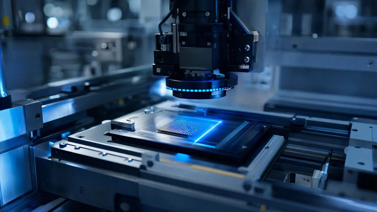
DaoAI 3D ACI equipment (featuring proprietary 3D camera + 3D morphology reconstruction/point cloud, detecting hidden solder joints/coplanarity/micron-level morphology/pores, and other 2D optical blind spot defects, with 2D-3D fusion) leverages high-resolution 3D imaging combined with deep learning algorithms to accelerate semiconductor micro-bump missing/bridging defect detection to 1.4 times the speed of traditional solutions, while reducing the false negative rate to <0.3%, effectively resolving both the capacity bottleneck and quality challenges of 100% full inspection on high-throughput production lines.
The semiconductor industry, as the core of modern information technology, has manufacturing processes whose precision directly determines chip performance and reliability. In advanced packaging, micro-bumps serve as critical connections between chips and substrates, with their quality directly impacting the electrical performance and long-term stability of the final product. As chip integration continues to increase, micro-bump sizes are shrinking and pitches are becoming tighter, posing unprecedented challenges for inspection technology. Especially on high-throughput mass production lines, achieving 100% full inspection of micron-level or even sub-micron micro-bump defects (such as missing, bridging, collapse, height inconsistency, etc.) without slowing down the overall production line throughput is a common challenge for semiconductor manufacturers. Traditional 2D optical inspection, limited by its imaging principles, has inherent blind spots when dealing with 3D morphological defects, making it difficult to accurately determine the true height, volume, and coplanarity of micro-bumps, leading to high false negative rates or frequent false alarms, severely impacting production line efficiency and product yield.
Pain Points: The Contradiction Between Production Throughput and 100% Full Inspection Capacity
In the micro-bump inspection stage of semiconductor advanced packaging, customers face multiple pain points: First, [inspection efficiency bottlenecks]. Traditional 2D AOI or manual visual inspection solutions have long inspection times per chip, making it difficult to meet production line throughputs of several or even dozens of chips per second. This prevents 100% full inspection, forcing reliance on sampling inspection, which carries potential quality risks. Second, [high false negative and false positive rates]. For subtle 3D defects such as missing or bridged micro-bumps, traditional 2D images lack sufficient depth information, leading to false negative rates as high as 0.8%~1.5%, while false positive rates can exceed 5%. A large number of good products are misjudged, increasing the burden of manual re-inspection. Third, [high cost of manual re-inspection]. High false positive rates mean significant human resources are needed for secondary confirmation; a skilled worker can only re-inspect a few hundred chips per day, leading to significantly increased labor costs and inconsistent inspection results due to subjective factors. Fourth, [long changeover times]. When product models or process parameters change, traditional AOI requires several hours or even half a day for parameter adjustment and programming, severely impacting production line utilization. These issues collectively lead to increased overall production costs and reduced market competitiveness, running counter to the current trend of AI inspection large models achieving hundreds of millions in cost savings in display panel manufacturing, highlighting the limitations of traditional solutions in high-precision, high-throughput quality inspection for semiconductors.
The root cause of these difficulties lies in the physical characteristics of micro-bump defects and the challenges of imaging. Micro-bump sizes typically range from tens to hundreds of microns, with height, volume, and morphology being critical quality indicators. 2D optical imaging can only acquire planar information, with limited ability to identify defects like height collapse or sidewall bridging. Furthermore, micro-bump surfaces may exhibit complex optical phenomena such as reflections and shadows, further interfering with 2D image analysis. In high-throughput production lines, to ensure inspection speed, image acquisition time is compressed, reducing the signal-to-noise ratio and making tiny defects harder to capture. Additionally, traditional rule-based algorithms struggle to adapt to the subtle variations and diversity of micro-bump morphology, resulting in poor model generalization and requiring frequent parameter adjustments, preventing intelligent defect recognition and classification.
Technical Principles: 3D ACI's Depth Perception and Intelligent Decision-Making
DaoAI's 3D ACI equipment fundamentally solves the problem of missing depth information in micro-bump inspection through its core proprietary 3D camera and 3D morphology reconstruction technology. The equipment employs a combination of multi-frequency structured light projection and phase-measuring profilometry (PMP) to rapidly acquire multiple images of the chip surface. Complex algorithms then reconstruct high-precision 3D point cloud data at a sub-microsecond level. This point cloud data contains the X, Y, Z 3D coordinate information of each micro-bump, accurately restoring its true morphology, height, volume, and coplanarity. Based on this rich 3D data, the DaoAI ACI OS further integrates advanced deep learning algorithms, specifically for 3D point cloud feature extraction and defect classification models. These models, trained on a large number of good and typical defect samples, can autonomously learn and identify various complex micro-bump defect patterns, such as precisely identifying collapsed bumps below a certain height threshold, bridged bumps exceeding a width threshold, and void areas of missing bumps, thereby achieving high-precision, robust defect detection.
Compared to traditional methods, the advantages of DaoAI's 3D ACI are significant. Traditional 2D AOI relies on 2D features like edges and textures from grayscale or color images, which are almost ineffective for defects lacking height information and are susceptible to factors like lighting and reflections. Manual visual inspection, while capable of identifying complex defects, is slow, inconsistent, and costly, and impractical for high-throughput production lines. DaoAI's 3D ACI, by directly acquiring 3D morphological data, completely eliminates 2D optical blind spots. It can accurately measure critical parameters like micro-bump height and volume, and combines this with AI algorithms for intelligent decision-making, reducing the false negative rate to a level far below traditional solutions. Concurrently, its high-speed 3D data acquisition and processing capabilities ensure that it meets high-precision inspection requirements while matching or even exceeding production line throughput, achieving 100% full inspection capacity targets. For example, in a typical application scenario, DaoAI's 3D ACI equipment can complete full inspection at a speed of 20 chips per second, significantly higher than the 10-12 chips per second of traditional solutions.
Typical Application Scenarios
- **Micro-bump Missing Detection:** Before flip-chip packaging, detect if the required micro-bumps are present on the chip pads. The challenge lies in the small size of micro-bumps, the subtle difference from the surrounding background when missing, and the possibility of partial detachment rather than complete absence. DaoAI's 3D ACI, through 3D point cloud reconstruction, can precisely identify height anomalies in the pad area, accurately capturing even minor collapses or partial missing bumps.
- **Micro-bump Bridging Detection:** Detect if there is a short-circuit connection between adjacent micro-bumps. The challenge is that bridging can occur at the top, middle, or bottom of the bumps, with various connection morphologies. DaoAI's 3D ACI leverages its 3D morphology reconstruction capability to accurately measure the minimum distance between bumps and the morphology of the connected area, combining AI algorithms to determine if bridging exists, avoiding misjudgments caused by viewing angle or lighting issues in traditional 2D images.
- **Micro-bump Height Consistency and Coplanarity Detection:** Ensure that all micro-bumps' heights are within the allowed tolerance range and maintain good coplanarity, which is crucial for subsequent soldering quality. The challenge requires precise height measurement for each micro-bump and calculation of overall coplanarity deviation. DaoAI's 3D ACI can perform independent Z-axis height measurements for each micro-bump and conduct statistical analysis, quickly identifying chips with abnormal heights or out-of-spec coplanarity.
- **Micro-bump Collapse/Deformation Detection:** Detect if micro-bumps have abnormal morphology due to process issues, such as top collapse or sidewall tilt. The difficulty is that these defects are often micron-level morphological changes that are difficult to distinguish in 2D images. DaoAI's high-precision 3D reconstruction can capture these subtle morphological changes, identifying abnormal morphologies by comparing them with standard bump models.
Case Study: A Leading Semiconductor Packaging Manufacturer's Capacity Leap
A leading semiconductor packaging manufacturer faced severe challenges in micro-bump inspection on its high-density flip-chip production line. Due to massive chip shipments, the inspection speed of traditional 2D AOI equipment could not meet the production line throughput requirements, forcing a sampling inspection strategy. This resulted in hundreds of chips with micro-bump defects still flowing into downstream processes each month, leading to additional rework costs and customer complaint risks. Simultaneously, the false positive rate of traditional equipment was as high as 6%, requiring 3 skilled workers to perform 8 hours of manual re-inspection daily, leading to high labor costs. To address this dilemma, the manufacturer introduced DaoAI's 3D ACI equipment. In the initial phase, the DaoAI engineering team collaborated closely with the client. Through the DaoAI ACI OS, rapid modeling was achieved, completing preliminary training of the defect recognition model in 5 minutes using a small number of good samples (only 15 images). After approximately 2 weeks of continuous on-site data optimization and model iteration, DaoAI's 3D ACI equipment successfully achieved integration with the production line's MES system. After deployment, the equipment achieved 100% full inspection at a speed of 25 chips per second, significantly exceeding the client's original inspection capability of 15 chips per second. Concurrently, the false negative rate for micro-bump defects was consistently controlled at <0.2%, and the false positive rate was reduced by 85%, to just 0.9%. This drastically reduced the manual re-inspection workload; the original 3 re-inspection workers now only require 0.5 FTE to complete the task, greatly optimizing human resource allocation and significantly improving the overall quality level and capacity utilization of the production line.
DaoAI's 3D ACI equipment not only solved the precision challenge of micro-bump inspection but also, with its exceptional detection speed, provided 100% full inspection capacity assurance for high-throughput semiconductor production lines, achieving a dual breakthrough in quality and efficiency.
DaoAI Solutions and Products
DaoAI's core solution for semiconductor micro-bump inspection is its proprietary 3D ACI equipment. This equipment integrates DaoAI's independently developed high-speed, high-precision 3D camera, capable of completing 3D morphological data acquisition of chip surfaces in milliseconds, and performing real-time 3D point cloud reconstruction through its built-in edge computing unit. Its core DaoAI ACI OS provides powerful defect recognition capabilities. We employ deep learning-based visual foundation models, supporting APDT (Automatic Positive Defect Training) positive/few-shot learning mode, requiring only 1–20 good sample images to complete automatic programming and deployment of the inspection model within 5 minutes, greatly shortening changeover times from traditional hours to less than 10 minutes. For complex defects like missing or bridged micro-bumps, the system can effectively distinguish true defects from visual artifacts caused by process fluctuations through semantic false positive filtering mechanisms, further reducing false positive rates. Furthermore, DaoAI's 3D ACI equipment supports 100% local private deployment, with all inspection data processed within the customer's factory, ensuring data security and privacy. To further enhance inspection coverage, the equipment also supports a 2D-3D fusion inspection mode, combining 2D image texture and color information with 3D inspection to achieve more comprehensive defect recognition, such as supplementary detection of 2D feature defects like micro-bump surface oxidation or scratches. The DaoAI World world model serves as a unified foundation, ensuring knowledge transfer and continuous learning capabilities across different product models and defect types, allowing the system to continuously optimize as production line data accumulates, achieving cross-scenario generalization and performance improvement.
By deploying DaoAI's 3D ACI equipment, customers have realized significant business value. In terms of quality, the false negative rate for micro-bump defects has been reduced from the traditional 0.8%~1.5% to <0.3%, significantly improving product yield and end-customer satisfaction. In terms of efficiency, the inspection throughput has increased by over 40%, achieving 100% full inspection, eliminating quality risks associated with sampling, and significantly reducing manual re-inspection hours, cutting re-inspection labor costs by 80%. Concurrently, rapid changeover capability has reduced downtime from several hours to less than 10 minutes, effectively improving production line utilization. These quantified results not only lead to direct cost savings but also enhance the customer's market competitiveness in the field of high-end semiconductor manufacturing.
FAQ
How does DaoAI's 3D ACI equipment ensure high throughput and 100% full inspection capacity for semiconductor production lines?
DaoAI's 3D ACI equipment, utilizing its proprietary high-speed 3D camera and optimized 3D morphology reconstruction algorithms, achieves millisecond-level 3D data acquisition and processing. Combined with an efficient deep learning inference engine, it ensures that while meeting sub-micron defect detection precision, the inspection speed significantly surpasses traditional solutions, thereby enabling semiconductor production lines to achieve 100% full inspection without impacting overall throughput, effectively enhancing capacity utilization.
Compared to traditional 2D AOI, what unique advantages does DaoAI's 3D ACI offer for detecting semiconductor micro-bump defects?
Traditional 2D AOI cannot acquire depth information, leading to blind spots for micro-bump height, volume, coplanarity, and sidewall defects. DaoAI's 3D ACI, through 3D point cloud reconstruction, accurately restores the true 3D morphology of micro-bumps, enabling the identification of 2D optical blind spot defects such as collapse and bridging. Combined with AI algorithms for intelligent judgment, it significantly reduces false negative and false positive rates, providing more comprehensive and reliable inspection results.
What is the typical cost structure and ROI period for deploying DaoAI's 3D ACI equipment?
The cost of DaoAI's 3D ACI equipment primarily includes hardware, software licensing, implementation services, and post-maintenance. Specific pricing varies based on factors such as production line scale, required inspection precision, and integration complexity. However, due to its significant reduction in false negative and false positive rates, decreased manual re-inspection costs, and improved production line throughput and yield, ROI is typically achieved within 6-18 months. We recommend contacting our sales team for a customized solution and detailed quotation.
This article was generated by AI. Customer cases are simulated scenarios based on real product capabilities and figures are illustrative; see product pages for official benchmarks.