
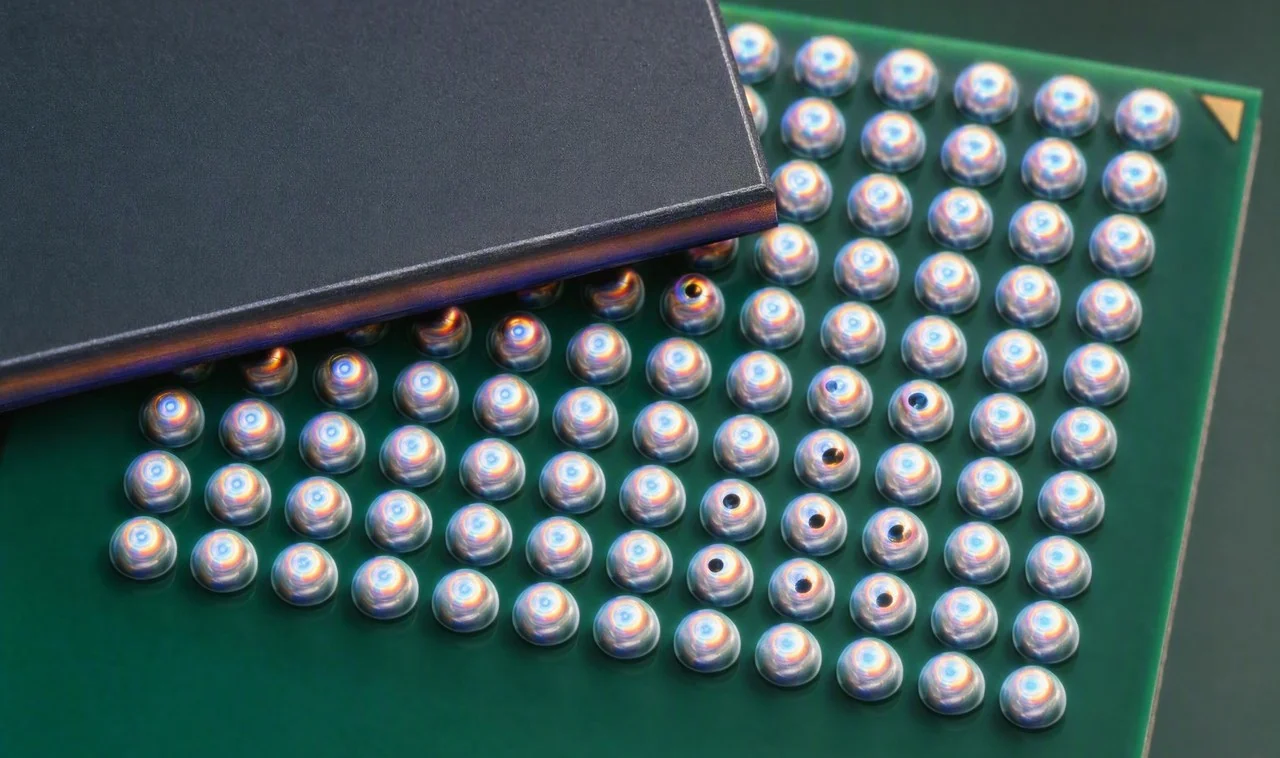
DaoAI 3D AI AOI equipment (proprietary 3D camera + 3D morphology reconstruction/point cloud, detecting hidden solder joints/coplanarity/micron-level morphology/voids and other 2D optical blind spot defects, 2D-3D fusion) leverages deep learning algorithms and precise 3D imaging to reduce the missed detection rate of BGA solder voids in the PCBA industry from 1.2% in traditional solutions to <0.4%, ensuring the long-term reliable operation of complex electronic products. In electronics/PCBA manufacturing, BGA (Ball Grid Array) packages are widely used in various motherboards, modules, and chipsets due to their high density and high performance. However, this packaging form also presents unique quality control challenges, especially internal voids in solder joints, which pose potential threats to product performance and lifespan. A leading PCBA manufacturer, producing complex motherboards for high-end servers and network equipment, was facing severe challenges in BGA solder void detection.
In electronics/PCBA manufacturing, BGA (Ball Grid Array) packages are widely used in various motherboards, modules, and chipsets due to their high density and high performance. However, this packaging form also presents unique quality control challenges, especially internal voids in solder joints, which pose potential threats to product performance and lifespan. A leading PCBA manufacturer, producing complex motherboards for high-end servers and network equipment, was facing severe challenges in BGA solder void detection. These voids not only affect electrical conductivity and heat dissipation but can also lead to solder joint cracking under extreme operating conditions, causing product failure. Traditional detection methods often struggle with BGA solder voids, failing to meet high detection rate requirements, which introduces significant risks to product reliability.
Pain Points: Why BGA Solder Voids Are So Difficult to Detect
The difficulty in detecting BGA solder voids primarily stems from several dimensions: first, detection blind spots, as traditional 2D optical inspection cannot penetrate the solder surface to detect internal voids; second, the limitations of X-ray image analysis. Although X-ray can see inside solder joints, its 2D projection image lacks precision in determining the 3D shape, depth, and position of voids, being susceptible to projection angles and void overlaps, leading to a prevalent missed detection rate of 1.2%. Furthermore, traditional X-ray equipment also has a higher false positive rate, typically between 5% and 8%, resulting in substantial manual re-inspection workload, averaging 3-4 hours of manual review daily, severely impacting production line takt time and efficiency. Similar to the industry trend in precision gear manufacturing where optical measurement offers superior accuracy and efficiency compared to contact measurement, BGA solder void detection also requires a shift from traditional X-ray's 'contact' or 'indirect' inspection to more precise and efficient optical 3D inspection to overcome its inherent limitations. The root causes of these void defects are complex, potentially originating from solder paste printing quality, improper reflow oven temperature profiles, or incomplete flux volatilization.
More challenging is the vast number of BGA solder joints; a single PCBA board can integrate thousands of BGA solder joints, and any tiny void can become a potential hazard. In a high-speed production environment, achieving 100% accurate inspection for such a massive number of solder joints is a significant challenge for any detection technology. While traditional X-ray equipment provides radiographic images, its image processing mainly relies on thresholding and simple geometric rules, making it difficult to effectively distinguish real voids from image noise, and unable to precisely quantify void volume and morphology, leading to persistent missed detections and false positives. DaoAI understands these pain points and is committed to breaking through these bottlenecks with innovative 3D AI AOI technology.
Technical Principles: How 3D AI AOI Precisely Identifies BGA Solder Voids
The core of DaoAI 3D AI AOI equipment lies in its proprietary 3D camera and advanced 3D morphology reconstruction algorithms, combined with deep learning models, to achieve precise detection of BGA solder voids. Unlike traditional X-ray which only provides 2D projections, DaoAI's 3D camera captures complete 3D morphological data of solder joints, generating high-precision point cloud models. Through multi-view structured light projection and image acquisition, the system can accurately restore the internal geometric structure of solder joints, including the shape, size, position, and depth of voids. This 3D data provides significantly more information than 2D images, allowing AI models to understand the true internal conditions of solder joints more comprehensively and accurately. Compared to traditional X-ray, which relies on human interpretation or simple threshold-based rule algorithms, DaoAI 3D AI AOI employs deep learning algorithms that can learn and identify complex void features from vast amounts of 3D data, effectively distinguishing real defects from normal morphology caused by process variations, thereby reducing the missed detection rate to <0.4%.
Furthermore, DaoAI's 2D-3D fusion technology is a key advantage. While acquiring 3D morphological data, the system also collects high-resolution 2D images. AI algorithms can simultaneously analyze 2D texture information and 3D morphological information, performing multi-modal feature fusion to compensate for the deficiencies of single-dimension information. For example, 2D images can assist in determining surface defects like oxidation or contamination, while 3D data focuses on internal voids. This fusion mechanism greatly enhances detection robustness and accuracy. Additionally, the DaoAI AI AOI software system features APDT positive/few-shot learning capabilities, requiring only 1–20 good samples for model training, which drastically shortens changeover time from hours to less than 5 minutes, significantly boosting production efficiency. This rapid changeover capability makes DaoAI 3D AI AOI highly adaptable to high-mix, low-volume production scenarios.
Typical Application Scenarios
- Internal Void Detection in BGA Solder Joints: Utilizing 3D morphology reconstruction, DaoAI 3D AI AOI can precisely identify bubbles, gaps, and other defects within solder balls, especially tiny voids hidden deep inside solder balls, which are blind spots for traditional 2D optical inspection and prone to missed detection by X-ray due to its 2D projection limitations.
- BGA Solder Joint Coplanarity and Height Consistency Detection: Through high-precision 3D point cloud data, DaoAI 3D AI AOI can measure the overall coplanarity of BGA solder ball arrays and the height differences of individual solder balls, ensuring welding quality and preventing risks of opens or shorts. Traditional methods struggle with non-contact, high-precision full-array coplanarity measurement.
- BGA Solder Joint Bridging and Open Circuit Detection: Combining 2D-3D fusion technology, DaoAI 3D AI AOI can not only use 2D images to determine abnormal connections (bridging) between solder joints but also use 3D morphology to determine if solder joints are completely detached (open circuits), addressing challenges faced by traditional 2D AOI in identifying tiny bridges and defects between high-density pads.
- Micron-level Solder Paste Volume and Shape Inspection: In the solder paste printing process before BGA packaging, DaoAI 3D AI AOI can perform micron-level volume, height, shape, and offset inspection of printed solder paste, preemptively detecting printing defects and preventing subsequent void formation during reflow soldering. This is crucial 3D information that traditional 2D AOI cannot provide.
- QFN Package Bottom Solder Joint Inspection: The thermal pads at the bottom of QFN (Quad Flat No-lead) packages are also prone to voids or cold solder joints. DaoAI 3D AI AOI can penetrate the edges of the package, using its 3D reconstruction capabilities to perform non-destructive inspection of bottom solder joints, compensating for deficiencies in traditional inspection.
Case Study: BGA Void Detection Revolution at a Leading PCBA Manufacturer
A leading PCBA manufacturer, a global supplier of server motherboards, had long been plagued by high missed detection rates and false positives caused by BGA solder voids. Their original production line relied on high-end X-ray equipment for BGA void detection, but due to the complexity of X-ray image interpretation and reliance on human experience, the actual missed detection rate was around 1.2%, leading to reduced product yield and potential market recall risks. At the same time, at least 3 experienced engineers were required daily for up to 4 hours of manual re-inspection, incurring high labor costs and low efficiency. After learning about DaoAI 3D AI AOI equipment's leading technology, the manufacturer decided to pilot its introduction. The DaoAI technical team integrated the 3D AI AOI system with the client's existing MES system via SDK without altering the current production line layout, and quickly completed model training and deployment. Before implementation, the client needed over 100 defect samples to train a barely usable X-ray image recognition model, whereas the DaoAI AI AOI software system, with its APDT positive/few-shot learning capability, completed initial model training with only 15 good samples, further improving performance in subsequent optimizations.
DaoAI 3D AI AOI helps with BGA void detection, reducing missed detection rates from 1.2% to <0.4%, false positive rates by −70%, and manual re-inspection hours by −85%.
After deployment, the performance of DaoAI 3D AI AOI equipment exceeded the client's expectations. Through its proprietary 3D camera and 3D morphology reconstruction technology, the system precisely identified and quantified tiny voids within BGA solder joints, successfully reducing the BGA solder void missed detection rate from 1.2% to <0.4%. Concurrently, thanks to deep learning algorithms' precise recognition of complex features, the false positive rate was also significantly reduced by 70%, from the previous 5%–8% to <2%. This led to a substantial reduction in manual re-inspection workload, with daily manual re-inspection hours decreasing by 85%, greatly freeing up engineers' productivity and accelerating product release times. The client's representative stated that DaoAI 3D AI AOI not only resolved long-standing quality pain points but also significantly improved production line automation and overall efficiency.
DaoAI Solutions and Products
The core solution provided by DaoAI for BGA solder void detection in the PCBA industry is its 3D AI AOI equipment. This device integrates DaoAI's proprietary high-precision 3D camera and a powerful 3D morphology reconstruction module, capable of acquiring complete point cloud data and high-resolution 2D images of solder joints. On the software side, the DaoAI AI AOI software system, serving as its intelligent brain, boasts the capability of "one good sample, 5 minutes, 0 code automatic programming," greatly simplifying model deployment and maintenance. Its APDT positive/few-shot learning feature requires only 1–20 good samples to initiate learning, significantly reducing changeover time and production line downtime. For BGA voids, the system analyzes density changes and geometric features in 3D morphological data, combined with surface information from 2D images, to achieve 2D-3D fusion detection, precisely identifying and quantifying void defects. The entire system supports 100% on-premises private deployment, ensuring client data security and compliance with high data privacy standards.
Through the application of DaoAI 3D AI AOI equipment, clients not only achieved a significant reduction in BGA solder void missed detection rates, ensuring product quality reliability, but also substantially reduced manual re-inspection efforts, enhancing production line automation. This technological advantage allows DaoAI to deliver tangible business value to clients in the field of precision inspection within the PCBA industry. The DaoAI World model, as a unified foundation, with its semantic understanding and cross-scenario generalization capabilities, also lays the groundwork for intelligent upgrades in more complex future detection scenarios, enabling production lines to continuously learn and optimize from feedback.
FAQ
What is the fundamental difference between DaoAI 3D AI AOI equipment and traditional X-ray for BGA void detection?
DaoAI 3D AI AOI equipment utilizes a proprietary 3D camera and 3D morphology reconstruction technology to directly acquire complete 3D data of solder joints, accurately quantifying the shape, volume, and position of voids. Traditional X-ray, however, only provides 2D projection images, which have blind spots and limitations in judging 3D voids, susceptible to angle and overlap issues, leading to higher missed detection rates. DaoAI achieves more comprehensive and precise inspection results through 2D-3D fusion.
How long does it take to deploy DaoAI 3D AI AOI equipment? Does it require extensive modifications to existing production lines?
DaoAI 3D AI AOI equipment supports flexible deployment methods, such as rapid integration with existing MES systems via SDK/API/Docker. Its APDT positive/few-shot learning capability typically requires only 1–20 good samples for initial model training, significantly shortening deployment time. In most cases, extensive modifications to existing production lines are not required, making the deployment process efficient with minimal impact on production.
How can I estimate the cost budget for DaoAI 3D AI AOI equipment?
The cost of DaoAI 3D AI AOI equipment depends on specific configuration requirements, such as inspection speed, precision level, integration complexity, and desired additional features. To provide the most accurate budget estimate, we recommend contacting our sales and technical team directly. We will provide a customized solution and detailed quotation based on your specific production line conditions and inspection needs.
Full solution for this scenario: Electronics / PCBA industry solutions
This article was generated by AI. Customer cases are simulated scenarios based on real product capabilities and figures are illustrative; see product pages for official benchmarks.