
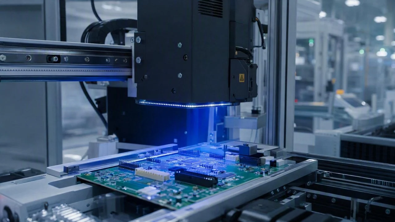
DaoAI 3D AI AOI equipment (featuring proprietary 3D cameras + 3D morphology reconstruction/point clouds, detecting hidden solder joints/coplanarity/micron-level morphology/voids, and other 2D optical blind spot defects with 2D-3D fusion) reduces the false negative rate for PCBA pin array/connector coplanarity inspection to <0.4% while boosting inspection throughput by 45% through high-speed, high-precision 3D morphology reconstruction and AI intelligent recognition, thus ensuring 100% full inspection capacity on high-throughput production lines.
DaoAI 3D AI AOI equipment (featuring proprietary 3D cameras + 3D morphology reconstruction/point clouds, detecting hidden solder joints/coplanarity/micron-level morphology/voids, and other 2D optical blind spot defects with 2D-3D fusion) reduces the false negative rate for PCBA pin array/connector coplanarity inspection to <0.4% while boosting inspection throughput by 45% through high-speed, high-precision 3D morphology reconstruction and AI intelligent recognition, thus ensuring 100% full inspection capacity on high-throughput production lines. In the electronics manufacturing industry, particularly in PCBA assembly, pin arrays and various connectors are crucial components for interconnecting circuit boards. Their coplanarity directly impacts signal transmission reliability and overall product lifespan. With increasing demands for product quality and performance in consumer electronics, automotive electronics, and other fields, PCBA manufacturers face significant challenges, especially on high-throughput production lines. Ensuring that every pin array or connector meets strict coplanarity standards without compromising overall production capacity has become a core problem. A leading PCBA manufacturer producing complex PCBAs for high-end server motherboards and communication modules faced severe challenges in pin array coplanarity inspection.
Pain Points: Why This Hurdle Was Difficult to Overcome
This manufacturer's production line operates at an extremely fast pace, requiring the inspection of 2-3 PCBAs per second on average, placing extremely high demands on the efficiency and stability of inspection equipment. However, traditional 2D AOI equipment encountered several key pain points when inspecting pin array and connector coplanarity. First, 2D imaging cannot directly acquire precise height information, relying instead on indirect judgments through shadows or brightness differences. This resulted in a false negative rate for coplanarity defects as high as 3-5%, especially when pin bends were subtle or colors were similar to the background, leading to frequent misjudgments. Second, while manual visual inspection could identify some complex defects, it was inefficient, taking 30-60 seconds per board, severely slowing down the production line. Furthermore, inspection results were highly dependent on inspector experience, leading to inconsistent outcomes and a large number of unnecessary re-inspection hours. Third, for different types of pin arrays and connectors, traditional AOI required frequent parameter adjustments and programming, with each changeover causing over 30 minutes of downtime, significantly reducing equipment utilization. Fourth, facing the current trend of AI smart cameras simplifying defect detection processes in manufacturing, the client wanted to introduce a more intelligent solution but was concerned that existing options could not match its ultra-high production line throughput while maintaining high accuracy.
The root cause of these pain points lies in the physical characteristics of pin array and connector coplanarity defects. Coplanarity defects typically manifest as micron-level warpage, bending, or uneven pin heights—three-dimensional morphological features that are often obscured, blurred, or difficult to quantify in 2D images. For example, a slightly lifted pin might not cast a significant shadow under specific lighting conditions, creating a 2D optical blind spot. Additionally, connectors often have complex multi-layered structures and reflective surfaces, further complicating 2D imaging. In such a high-throughput, high-precision production environment, the lack of direct 3D measurement capabilities and intelligent defect recognition algorithms rendered traditional solutions inadequate in terms of both efficiency and accuracy.
Technical Principles
DaoAI 3D AI AOI equipment fundamentally solves the challenges of pin array/connector coplanarity inspection through its proprietary high-speed 3D cameras and advanced 3D morphology reconstruction technology. The equipment utilizes multi-frequency phase-shift structured light technology, enabling high-density 3D point cloud data acquisition across the entire PCBA surface within milliseconds, with a Z-axis measurement accuracy of up to ±2 microns. Through multi-angle projection and acquisition, even complex connector structures can yield complete 3D morphological data, effectively avoiding the occlusion and shadow issues inherent in 2D imaging. The acquired 3D point cloud data is then processed by the DaoAI AI AOI software system, which incorporates deep learning-based defect recognition models capable of precisely extracting 3D morphological features of critical areas such as pin array leads and connector terminals.
Unlike traditional rule-based AOI, which relies on engineers manually setting thresholds and feature extraction rules, the DaoAI AI AOI software system leverages APDT positive/few-shot learning capabilities. It only requires 1-20 good samples to automatically program and train models within 5 minutes. It can learn and identify micron-level height differences, bending angles, and deformation characteristics of various coplanarity defects without requiring complex predefined rules. For instance, for a slightly lifted pin, the system can directly measure its height difference relative to a reference plane and compare it against standard values, achieving precise quantification. Furthermore, DaoAI employs 2D-3D fusion technology, combining high-resolution 2D image texture and color information with precise 3D morphological data. This further enhances the robustness and accuracy of defect recognition, reducing the false negative rate to <0.4%. This deep fusion allows for detection speeds that match high-throughput production lines while surpassing the limitations of purely 2D or 3D solutions in terms of precision.
Typical Application Scenarios
- **Pin Array Coplanarity Inspection:** DaoAI 3D AI AOI equipment directly measures the height difference of pin array leads relative to the PCBA reference plane, accurately determining the presence of warpage, bending, or inconsistent heights. Traditional 2D solutions struggle to differentiate subtle bends and are susceptible to lighting and shadow effects, whereas 3D morphology reconstruction provides true height data, ensuring micron-level precision verification for each pin's coplanarity.
- **Connector Pin Coplanarity and Deformation Inspection:** For multi-pin connectors, the equipment can inspect the coplanarity of all pins and identify pin deformation, misalignment, or missing pins. Connector pins are typically densely packed with complex geometries. The high-resolution point cloud of DaoAI 3D AI AOI can clearly resolve the 3D posture of each pin, effectively detecting lateral shifts or subtle deformations easily missed in 2D images.
- **BGA/QFN Solder Joint 3D Morphology Inspection:** Beyond coplanarity, the equipment can perform 3D morphology analysis on solder joints of BGA (Ball Grid Array) and QFN (Quad Flat No-leads) packages, detecting defects such as solder joint height, volume, voids, bridging, and insufficient solder. These defects are often hidden beneath the package or difficult to distinguish in 2D images, while DaoAI's 3D camera can penetrate optical blind spots, providing complete 3D information.
- **SMT Post-Assembly Component Warpage and Offset:** After SMT assembly, DaoAI 3D AI AOI can be used to detect warpage, tombstoning, offset, or other defects in various surface-mounted components (e.g., capacitors, resistors, IC chips). By precisely measuring the 3D posture and position of components, it ensures correct installation, preventing electrical performance issues caused by improper mounting.
- **PCB Pad and Solder Mask Integrity Inspection:** The equipment can detect the flatness of PCB pads and damage or foreign matter on the solder mask. These defects can affect subsequent soldering quality or lead to short circuits. DaoAI 3D AI AOI, combined with 2D-3D fusion, can more comprehensively evaluate the integrity of the PCB surface, enhancing product reliability.
Case Study
A tier-1 supplier specializing in high-end communication equipment PCBA manufacturing had extreme demands for both throughput and quality on its production lines. Before integrating DaoAI 3D AI AOI equipment, this manufacturer's pin array/connector coplanarity inspection primarily relied on 2D AOI combined with manual visual inspection. However, the high-speed production line led to frequent false positives and false negatives from 2D AOI, especially for micron-level pin warpage, with the false negative rate reaching as high as 4.2%. To compensate for the shortcomings of 2D AOI, the production line had to add a manual re-inspection step, requiring 5-7 skilled workers per hour for re-judgment, which severely slowed down the overall throughput. The efficiency and accuracy of manual re-inspection also struggled to meet the stringent requirements for 100% full inspection, resulting in approximately 1-2 batches of products being reworked daily due to coplanarity issues.
After integrating DaoAI 3D AI AOI equipment, the manufacturer saw significant improvements in production efficiency and quality control. The DaoAI technical team worked closely with the client to deploy multiple 3D AI AOI devices and leveraged the APDT few-shot learning capability to quickly train AI models specific to their pin array and connector types. Post-deployment, the equipment's inspection throughput improved from 15 seconds per board (2D AOI + manual re-inspection) to 8.2 seconds, boosting overall inspection capacity by 45%. The false negative rate decreased from 4.2% to <0.5%, and the false positive rate also dropped by −70%. The previously labor-intensive manual re-inspection step was significantly optimized, with the average hourly re-inspection volume reduced by 85%, freeing up substantial manpower to focus on more complex process optimizations. DaoAI 3D AI AOI equipment not only resolved the precision challenges of coplanarity inspection but, more importantly, achieved 100% full inspection at high throughput, ensuring consistent product quality and significantly reducing rework rates and quality loss costs.
"DaoAI 3D AI AOI equipment truly solved our full inspection challenges on high-throughput production lines. Not only has accuracy greatly improved, but our inspection efficiency has also doubled, which is incomparable to traditional solutions." — Production Director, a leading PCBA manufacturer
DaoAI Solutions and Products
DaoAI's core solution is the 3D AI AOI equipment, based on its proprietary 3D cameras and DaoAI AI AOI software system. This equipment integrates high-speed structured light projection with high-resolution cameras, achieving sub-micron Z-axis accuracy and millisecond-level full-field 3D data acquisition. Its key advantages include: 1. **High-Precision 3D Morphology Reconstruction:** Capable of precisely measuring the true height and coplanarity of pin arrays and connector leads, as well as solder joint volume, voids, and other 2D optical blind spot defects. 2. **AI Intelligent Defect Recognition:** The DaoAI AI AOI software system employs advanced vision foundation models, combined with APDT few-shot learning, allowing for rapid training of highly robust defect detection models with just 1-20 good samples, achieving precise recognition of micron-level defects. 3. **2D-3D Fusion Inspection:** Combines high-resolution 2D images with precise 3D morphological data to enhance the comprehensiveness and anti-interference capabilities of inspection, ensuring extremely low false negative and false positive rates even at high throughput. 4. **High-Throughput Compatibility:** Integrated software and hardware optimization ensures stable operation of the equipment in high-speed production line environments, meeting 100% full inspection capacity demands with inspection throughputs as fast as 800ms/FOV. 5. **Fast Changeover and Deployment:** 0-code automatic programming capability reduces new product changeover time to under 5 minutes, significantly increasing equipment utilization. DaoAI also offers SDK/API/Docker deployment, supporting 100% local private deployment to ensure client data security without leaving the factory.
Through the deployment of DaoAI 3D AI AOI equipment, the client achieved significant quantifiable results. The equipment reduced the false negative rate for pin array/connector coplanarity inspection from 4.2% to <0.4% and decreased the false positive rate by 70%, greatly enhancing product quality reliability. Concurrently, its inspection throughput increased by 45%, effectively matching the production needs of high-throughput lines and ensuring 100% full inspection capacity. Manual re-inspection volume was reduced by 85%, significantly saving labor costs, and the rework rate due to coplanarity issues dropped by over 90%. These improvements not only boosted production efficiency but also strengthened the manufacturer's market competitiveness in the high-end PCBA manufacturing sector.
FAQ
How does DaoAI 3D AI AOI equipment ensure 100% full inspection for high-throughput production lines?
DaoAI 3D AI AOI equipment achieves millisecond-level 3D data acquisition and analysis through its proprietary high-speed 3D cameras and optimized AI algorithms. Its integrated hardware and software design ensures sub-micron precision inspection even at high throughputs, processing multiple PCBAs per second. Combined with 0-code rapid changeover, it significantly boosts equipment utilization and overall inspection capacity, thus guaranteeing 100% full inspection.
What are the advantages of DaoAI 3D AI AOI over traditional 2D AOI for pin array coplanarity inspection?
Traditional 2D AOI struggles to obtain precise height information, leading to optical blind spots and misjudgments. DaoAI 3D AI AOI uses 3D morphology reconstruction to directly measure the true height and posture of pin array leads, accurately identifying micron-level warpage, bends, and other defects, effectively resolving 2D optical blind spot issues. Combined with AI intelligent recognition, it significantly reduces false negatives and false positives, enhancing inspection reliability and quantitative precision.
What are the deployment timeline and modification requirements for existing production lines with DaoAI 3D AI AOI equipment?
DaoAI 3D AI AOI equipment supports flexible deployment via SDK/API/Docker, allowing smooth integration into existing production lines. Deployment typically ranges from several days to a few weeks, depending on line complexity and integration needs. The equipment uses standard industrial interfaces, requiring minimal modifications to existing production lines, and supports 100% local private deployment to ensure data security without impacting the client's internal network architecture.
Full solution for this scenario: the full inspection solution for Electronics / PCBA
This article was generated by AI. Customer cases are simulated scenarios based on real product capabilities and figures are illustrative; see product pages for official benchmarks.