
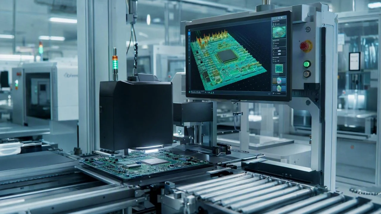
DaoAI 3D AI AOI equipment (proprietary 3D camera + 3D morphology reconstruction/point cloud, detecting hidden solder joints/coplanarity/micron-level morphology/voids and other 2D optical blind spot defects, 2D-3D fusion) precisely identifies hidden solder joint defects under BGA/QFN packages, reducing the missed detection rate for such defects from 1.2% to 0.08%, and establishes a complete quality traceability and data closed-loop system, significantly enhancing quality control capabilities in electronic product manufacturing.
DaoAI 3D AI AOI equipment (proprietary 3D camera + 3D morphology reconstruction/point cloud, detecting hidden solder joints/coplanarity/micron-level morphology/voids and other 2D optical blind spot defects, 2D-3D fusion) precisely identifies hidden solder joint defects under BGA/QFN packages, reducing the missed detection rate for such defects from 1.2% to 0.08%, and establishes a complete quality traceability and data closed-loop system, significantly enhancing quality control capabilities in electronic product manufacturing. In the electronics manufacturing industry, PCBAs (Printed Circuit Board Assemblies) are core components, and their quality directly determines the performance and reliability of end products. With the trend towards miniaturization and high integration of electronic products, advanced packaging technologies such as BGA (Ball Grid Array) and QFN (Quad Flat No-leads) are widely used. These packages feature solder joints hidden beneath or on the sides of the components, creating severe blind spots for traditional 2D optical inspection methods, making it difficult to effectively detect solder joint defects. A leading PCBA manufacturer, a global leader in electronic product contract manufacturing, processes millions of PCBAs daily on its production lines and has extremely high requirements for the quality of BGA/QFN solder joints. Especially in critical products like high-end smart devices and server motherboards, any minor solder joint defect can lead to product failure and even recall risks. Therefore, establishing an inspection system capable of precisely identifying hidden defects and achieving a quality data closed loop has become an urgent challenge for this manufacturer.
Pain Points: Why This Hurdle Was So Difficult to Overcome
Solder joint inspection for BGA/QFN packages presents multiple challenges, making traditional inspection solutions inadequate. Firstly, **high missed detection rates**: As solder joints are located beneath the components, traditional 2D AOI struggles to directly observe the complete morphology of solder joints through frontal optical imaging, leading to missed detection rates for open circuits, short circuits, cold solder joints, and voids exceeding 1.2%, severely impacting product reliability. Secondly, **inefficient and subjective manual re-inspection**: Suspicious defects require extensive manual X-Ray inspection or destructive analysis, which not only consumes a significant amount of time (averaging 5-8 minutes per PCBA for re-inspection) but also yields results influenced by operator experience, making consistency difficult to guarantee. Thirdly, **lack of effective data traceability mechanisms**: Traditional inspection data is often disparate and cannot be effectively linked with production batches, process parameters, raw material batches, and other information. This makes it difficult to quickly identify the root cause of batch defects and perform precise recalls once they are discovered, leading to high compliance risks, especially with increasingly stringent national and industry standards where data closed-loop becomes a mandatory requirement. Finally, **complex and difficult-to-quantify defect types**: Micron-level morphological changes in BGA solder joint collapse, bridging, tombstoning, and poor wetting of QFN side solder joints all exceed the detection capabilities of traditional 2D AOI and are difficult to accurately quantify using traditional rule-based algorithms. Aligning with the current trend of AI inspection large models achieving high-precision defect identification in display panel manufacturing, the PCBA industry also urgently needs to introduce more advanced AI vision technology to overcome these traditional bottlenecks.
The root cause of these dilemmas lies in: process-wise, the leadless or ball grid array design of BGA/QFN packages shields the solder joints; imaging-wise, 2D optical imaging is limited by perspective and cannot capture complete 3D morphological information of solder joints; material-wise, differences in reflective properties of various solders and fluxes also increase the complexity of 2D imaging; and takt time-wise, high-speed production lines demand inspection equipment to make precise judgments within extremely short periods, while traditional in-line X-Ray inspection is slow and cannot meet the requirements for 100% full inspection.
Technical Principles
DaoAI 3D AI AOI equipment, through its core proprietary 3D camera and 3D morphology reconstruction technology, fundamentally solves the challenge of hidden solder joint inspection under BGA/QFN packages. The equipment employs a multi-frequency structured light projection scheme, combined with high-precision industrial cameras, to capture multiple images of the PCBA surface at different phases. These images are processed by DaoAI's unique 3D morphology reconstruction algorithms, which can accurately restore micron-level 3D point cloud data of the solder joints. By performing deep learning analysis on this point cloud data, the DaoAI AI AOI software system can precisely extract key 3D features of solder joints, such as volume, height, coplanarity, and void ratio. For instance, for BGA solder joints, it can accurately measure the degree of collapse of each solder ball, whether the solder volume is sufficient, and if bridging exists; for QFN side solder joints, it can detect solder paste height and wetting angle, identifying cold solder joints or poor wetting. DaoAI 3D AI AOI's 2D-3D fusion technology further combines texture and color information from 2D images, complementing the limitations of single-dimension detection, making defect identification more comprehensive and robust.
Compared to traditional rule-based AOI, the advantage of DaoAI 3D AI AOI lies in its intelligent recognition capabilities based on deep learning. Traditional rule-based AOI relies on manually set thresholds and geometric rules, which have poor adaptability to complex and varied defect types, often leading to a large number of false positives and missed detections. In contrast, the DaoAI AI AOI software system, through its APDT positive/few-shot learning technology, can quickly train high-precision models with just 1-20 good samples, adapting to various process fluctuations and material differences. Compared to traditional in-line X-Ray inspection, DaoAI 3D AI AOI offers higher inspection speed and non-destructive testing. While X-Ray can penetrate components, its high cost, radiation safety concerns, and relatively slow inspection takt time make it difficult to achieve 100% full inspection on all production lines. DaoAI 3D AI AOI, with its sub-micron level detection accuracy and high-speed processing capability, achieves online, non-contact full inspection of BGA/QFN solder joint defects, and can control the inspection takt time within 300ms/FOV, significantly improving production efficiency.
Typical Application Scenarios
- **BGA Solder Ball Collapse and Bridging Detection**: After BGA package soldering, DaoAI 3D AI AOI equipment can precisely measure the height and diameter of each solder ball through 3D morphology reconstruction, identifying solder ball collapse, insufficient volume, or bridging defects caused by excessive solder. The challenge lies in the dense and tiny morphology of solder balls, which is difficult for traditional 2D to distinguish.
- **QFN Side Solder Joint Poor Wetting and Cold Solder Joints**: For QFN packages, solder joints are on the sides of the component. DaoAI 3D AI AOI uses lateral 3D imaging technology to detect solder paste height and wetting angle, identifying cold solder joints, poor wetting, insufficient solder, and other defects. The challenge lies in side solder joints being susceptible to shadows, and requiring extremely high precision in height measurement.
- **BGA Bottom Voids and Pores Detection**: Voids or pores within the solder are significant causes of BGA solder joint failure. DaoAI 3D AI AOI effectively identifies internal voids and pores by performing volume analysis on the solder joint's 3D point cloud data, combined with 2D-3D fusion judgment, and quantifies their size and location. The challenge is that voids are usually hidden inside the solder and have irregular shapes.
- **Coplanarity and Lead Warpage Detection**: Before or after BGA/QFN component placement, DaoAI 3D AI AOI can perform high-precision measurements of the coplanarity of component leads or solder ball arrays, identifying lead warpage or poor coplanarity to prevent open circuits or short circuits during placement. The challenge lies in precisely sensing micron-level flatness differences.
- **Solder Joint Volume and Consistency Analysis**: Analyze the volume consistency of BGA/QFN solder joints across the entire PCBA to ensure that the solder volume of each joint meets process requirements, preventing reliability issues caused by insufficient or excessive solder. The DaoAI software system can perform batch statistical analysis on all solder joints, providing critical data.
Case Study
A globally leading PCBA manufacturer, with its factory in South China, primarily produces high-end server motherboards. This factory faced challenges of high missed detection rates for BGA/QFN solder joint defects, heavy pressure from manual re-inspection, and a lack of effective quality traceability mechanisms. Previously, they relied mainly on traditional 2D AOI for initial inspection, supplemented by sampled X-Ray and extensive manual visual re-inspection. This approach resulted in a BGA solder joint missed detection rate as high as 1.2%, with weekly product rework costs due to missed detections exceeding hundreds of thousands of RMB. Furthermore, quality data for each PCBA batch could not be effectively linked to upstream process parameters, making root cause analysis difficult. To address this pain point, the manufacturer introduced DaoAI 3D AI AOI equipment. During the implementation, the DaoAI engineering team worked closely with the client, leveraging the APDT few-shot learning capability of the DaoAI AI AOI software system. In just one week, based on 15 good samples and a few defect samples provided by the client, they completed the rapid deployment and optimization of the BGA/QFN solder joint defect detection model. The integration of DaoAI 3D AI AOI equipment on the production line was also very smooth, achieving smooth integration with the factory's existing production management system via standard MES interfaces.
With DaoAI 3D AI AOI, we not only reduced the missed detection rate for hidden BGA/QFN solder joints to 0.08%, but more importantly, built a full-link quality data closed loop from inspection to traceability, which is a critical step towards our smart manufacturing.
After deployment, the DaoAI 3D AI AOI equipment performed exceptionally well. At the manufacturer's site, the missed detection rate for hidden solder joint defects (such as collapse, bridging, voids) under BGA/QFN packages significantly decreased from the original 1.2% to 0.08%, an increase of 93.3% in detection accuracy. Concurrently, due to the precision of 3D inspection, the false positive rate also decreased by 75%, significantly reducing the workload of manual re-inspection and freeing up 6 re-inspection operators. More critically, the DaoAI 3D AI AOI system uploads all solder joint inspection data, including 3D morphological features, defect types, and location information, in real-time to the client's MES system. Through the unified data foundation provided by the DaoAI World model, this data is linked with production batches, material batches, process parameters, and other information, forming a complete quality traceability chain. Now, if a downstream product issue is discovered, the client can quickly trace the data to pinpoint the affected batch range and potential causes, greatly improving problem response speed and recall efficiency, and providing data support for subsequent process optimization.
DaoAI Solution and Products
The core solution provided by DaoAI to this leading PCBA manufacturer is its proprietary 3D AI AOI equipment, which integrates a high-precision proprietary 3D camera and the powerful DaoAI AI AOI software system. In the modeling phase, DaoAI utilizes innovative APDT positive/few-shot learning technology, requiring only 1-20 good sample images to quickly establish BGA/QFN solder joint defect detection models, without the need for a large number of defect samples. This significantly shortens the model training cycle, reducing new product changeover time from several hours to 5min, greatly enhancing production line flexibility. For deployment, DaoAI 3D AI AOI equipment supports 100% on-premise private deployment, ensuring customer data security and local processing capabilities. The equipment integrates smoothly with the client's MES system via standard interfaces (such as SECS/GEM), enabling real-time upload of inspection data and two-way communication, establishing a complete data closed loop from inspection, analysis to traceability. Furthermore, the DaoAI World model serves as a unified AI foundation, enabling the system to continuously learn from production line feedback through semantic understanding and cross-scenario generalization, constantly optimizing detection accuracy and efficiency, and providing a solid foundation for the client's future smart factory upgrades. Through DaoAI Robot Vision's 6D pose recognition capabilities, it can further extend to automated rework and intelligent assembly guidance in the future, achieving more comprehensive smart manufacturing upgrades.
Through the DaoAI 3D AI AOI solution, the manufacturer not only achieved ultra-high precision detection of hidden BGA/QFN solder joint defects but also built a comprehensive quality traceability and data closed-loop system. This not only reduced the missed detection rate for hidden BGA/QFN solder joints to <0.08% and the false positive rate by −75%, but also brought significant business value: greatly improved product reliability and increased customer satisfaction; enhanced production efficiency and reduced manual re-inspection costs; most importantly, through data closed-loop, achieved end-to-end quality traceability from source to finished product, effectively avoiding potential quality risks and recall costs, providing a solid guarantee for the company's sustainable development. DaoAI is committed to helping electronic manufacturing enterprises achieve higher levels of intelligent production and quality management through leading AI vision technology.
FAQ
How does DaoAI 3D AI AOI enable quality traceability for solder joint defects?
DaoAI 3D AI AOI system collects 3D morphological data and defect information for each solder joint in real-time, linking it with critical production data such as PCBA batch, workstation, and operator. This structured data is uploaded to the client's MES/PLM system via standard interfaces, forming a traceable quality archive. When downstream product issues are discovered, a quick reverse lookup can pinpoint the root cause, enabling full lifecycle quality management and data closed-loop.
What are the advantages of DaoAI 3D AI AOI over traditional X-Ray inspection for BGA/QFN defect detection?
DaoAI 3D AI AOI offers non-destructive, high-speed, and cost-effective advantages. While X-Ray inspection can penetrate components, it is slower, unsuitable for 100% inline inspection, and involves radiation safety concerns and high equipment costs. DaoAI 3D AI AOI, through proprietary structured light and AI algorithms, achieves sub-micron 3D morphology reconstruction and defect recognition at high speeds, enabling 100% inline inspection without radiation risks, resulting in lower overall operating costs, making it more suitable for large-scale PCBA production lines.
How does DaoAI 3D AI AOI address the challenges of rapid product iteration in the PCBA industry?
The DaoAI AI AOI software system integrated with DaoAI 3D AI AOI features APDT positive/few-shot learning capabilities, allowing new models to be trained quickly with just 1-20 good samples, reducing new product changeover time to 5min. This rapid programming and adaptability enable the equipment to flexibly respond to the frequent product changeovers and rapid iteration demands of the PCBA industry, minimizing downtime and ensuring production efficiency.
Full solution for this scenario: the full inspection solution for Electronics / PCBA
This article was generated by AI. Customer cases are simulated scenarios based on real product capabilities and figures are illustrative; see product pages for official benchmarks.