
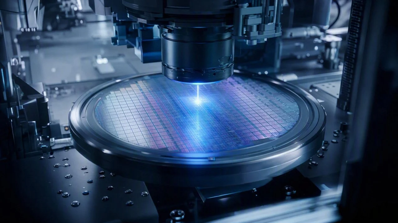
DaoAI 3D AI AOI equipment (proprietary 3D camera + 3D morphology reconstruction/point cloud, detecting hidden solder joints/coplanarity/micron-level morphology/voids and other 2D optical blind spot defects, 2D-3D fusion) achieves over 98% replacement of manual inspection for semiconductor pin coplanarity and dicing chipping through automated high-precision detection, effectively reducing production line labor costs and operational risks.
In the rapidly evolving semiconductor industry, pin coplanarity after chip packaging and dicing chipping defects after wafer cutting are critical factors affecting product reliability and yield. Traditionally, these micron-level fine defects have largely relied on intensive manual inspection by skilled workers. However, as chip integration increases and production cycles accelerate, the limitations of manual inspection are becoming increasingly apparent. It is not only inefficient and susceptible to subjective judgment but also leads to immense labor cost pressures and potential quality risks. Especially against the backdrop of rising labor costs, seeking efficient, precise, and quantifiable alternatives to manual inspection has become an urgent need for semiconductor manufacturers to reduce costs and enhance efficiency. DaoAI 3D AI AOI equipment is designed precisely to address this pain point, offering reliable automated inspection capabilities for the semiconductor industry by integrating 2D-3D vision technology.
Pain Points: Why This Hurdle is Difficult to Overcome
Semiconductor manufacturing faces multiple challenges in detecting pin coplanarity and dicing chipping. Firstly, there are **high labor costs and human resource bottlenecks**: A medium-sized packaging and testing production line typically requires dozens or even hundreds of experienced inspection workers operating in shifts to ensure the detection rate of pin coplanarity and dicing chipping defects. Annual labor costs can amount to tens of millions of RMB. As industry talent competition intensifies, the cost of recruiting and training qualified inspection personnel also rises, and high personnel turnover makes it difficult to effectively accumulate and pass on inspection experience. Secondly, **low inspection efficiency and cycle time limitations**: Manual inspection of a single chip typically takes 5-15 seconds. For production lines with millions of units per day, manual inspection has become a significant bottleneck, severely limiting the improvement of overall production cycle time. Moreover, long hours of intense, repetitive work easily lead to employee fatigue, further impacting inspection efficiency and accuracy. Thirdly, **high subjectivity and missed detection risks**: Pin coplanity deviation and dicing chipping are often micron-level or even sub-micron-level subtle defects. The human eye is prone to visual fatigue during prolonged observation, leading to consistently high missed detection rates for subtle defects, typically ranging from 3%–5% for traditional manual inspection. In addition, subjective judgment varies among different inspectors, resulting in poor consistency of inspection results, which is detrimental to quality traceability and statistical analysis. Finally, **2D vision blind spots and complex morphology challenges**: Pin coplanarity involves height differences in the Z-axis direction, and dicing chipping is a material loss in three-dimensional space. These defects are often inconspicuous or even in optical blind spots under traditional 2D vision, making them highly susceptible to misjudgment or missed detection. For example, slight pin bending or warping might only appear as blurred edges in a 2D image, making it difficult to precisely quantify its 3D morphology.
These fundamental issues place immense operational pressure on semiconductor manufacturers while ensuring product quality. Especially with the current trend of AI large models empowering industrial inspection, traditional manual inspection solutions are incompatible with automated, intelligent, and data-driven production models, urgently requiring the introduction of advanced inspection technologies to achieve both cost savings and accuracy improvements.
Technical Principles
The core advantage of DaoAI 3D AI AOI equipment lies in its **proprietary 3D camera and advanced 3D morphology reconstruction technology**. The equipment is equipped with a high-precision customized structured light or laser scanning 3D camera. By projecting specific light patterns or scan lines and capturing their deformation on the object's surface, it accurately reconstructs **high-density 3D point cloud data** of the inspected chip pins and dicing areas using triangulation principles or multi-view stereo matching algorithms. This point cloud data contains XYZ coordinate information for each point on the object's surface, thereby accurately reflecting the chip's 3D morphology. Unlike traditional 2D vision, which only captures planar grayscale or color information, DaoAI 3D AI AOI can directly quantify pin height differences, curvature, and the depth and width of dicing edge collapse, effectively avoiding missed detections caused by 2D optical blind spots.
Building upon this, DaoAI 3D AI AOI equipment integrates **advanced AI vision algorithms**. For pin coplanarity, the system can calculate the maximum height difference between the reference plane and the actual contact points of each pin based on the reconstructed point cloud data and compare it with preset tolerance ranges. For dicing chipping, the AI algorithm can precisely identify abnormal morphology at the dicing edge, such as collapse, nicks, or burrs, and quantify parameters like volume, depth, and area. Concurrently, the DaoAI AI AOI software system possesses powerful **2D-3D fusion detection capabilities**. It not only uses 3D data for morphological analysis but also combines high-resolution 2D images for auxiliary feature recognition like texture and color, achieving more comprehensive and robust defect detection. Compared to traditional rule-based AOI systems, the deep learning models employed by DaoAI 3D AI AOI can automatically learn defect features from vast amounts of data, maintaining a high detection rate even when facing complex and varied defect forms, reducing the missed detection rate to <0.5%. It also boasts stronger generalization and anti-interference capabilities. Compared to purely manual inspection, its detection accuracy and consistency have achieved a qualitative leap, reducing manual re-inspection hours by over 80%.
Typical Application Scenarios
- **Chip Package Pin Coplanarity Detection**: In package types like QFP, QFN, and BGA, DaoAI 3D AI AOI equipment can precisely measure pin flatness, bend, warp, and coplanarity, ensuring all pins are on the same plane to avoid bridging or short-circuit risks. The challenge lies in the numerous pins, tiny spacing, and extremely high Z-axis accuracy requirements.
- **Wafer Dicing Chipping Detection**: After the wafer dicing process, the equipment inspects the chip edges to identify chipping, cracks, or nicks caused during dicing. DaoAI 3D AI AOI can quantify the depth and width of chipping through 3D morphological data, preventing reduced chip strength or difficulties in subsequent packaging due to chipping. The challenge lies in the diverse forms of chipping and potential hiding within the kerf walls.
- **Micro-bump Height Consistency Detection**: In advanced packaging such as Flip-Chip, the height consistency of micro-bumps directly affects interconnection reliability. DaoAI 3D AI AOI equipment can accurately measure the height of each micro-bump, ensuring uniformity and identifying excessively high or low bumps. The challenge lies in the extremely small size of micro-bumps (typically tens of microns) and their vast number.
- **Mold Compound Morphology Defect Detection**: For the surface of the chip's mold compound after encapsulation, DaoAI 3D AI AOI can detect 3D morphological defects such as bubbles, depressions, scratches, and overflow. These defects can affect the chip's heat dissipation performance or reliability. The challenge lies in these defects often being micron-level, with potential reflections or texture interference on the surface.
- **Chip Size and Position Accuracy Measurement**: DaoAI 3D AI AOI equipment can perform high-precision measurements and positioning of the overall chip dimensions, pad locations, and character printing, ensuring the chip meets design specifications and providing precise positioning information for subsequent processes. The challenge lies in the high demands on equipment stability, calibration accuracy, and algorithm robustness for high-precision measurements.
Case Study
A leading domestic semiconductor packaging and testing manufacturer faced persistent challenges with manual inspection for pin coplanarity and dicing chipping on its high-end memory chip packaging lines. The manufacturer operated 5 production lines, each staffed with 15 inspection workers on three shifts, incurring annual manual inspection costs of nearly 20 million RMB. Due to the inefficiency of manual inspection, the inspection cycle time per chip was as long as 8-12 seconds, severely limiting production line capacity. Furthermore, the manual inspection missed detection rate hovered around 4%, leading to frequent customer complaints and high rework rates. To address this pain point, the manufacturer introduced DaoAI 3D AI AOI equipment for automation upgrade.
In the initial phase of the project, the DaoAI team conducted an in-depth analysis of the client's typical defect samples and utilized the DaoAI AI AOI software system for model training. Through the APDT few-shot learning capability, the core detection model was built and optimized within 5 days using only 15 good samples and a small number of defect images. After the equipment went online, at the manufacturer's site, DaoAI 3D AI AOI achieved an inspection cycle time of <200ms per chip, reducing the original inspection time by over 90% and increasing overall production line capacity by 30%. More importantly, the equipment successfully replaced over 95% of manual inspection positions, reducing the labor requirement per production line from 15 people to just 1-2 people responsible for equipment maintenance and abnormal re-inspection. This directly saved over 13 million RMB in annual labor costs, achieving a labor cost reduction of 65%. Simultaneously, the system's missed detection rate dropped to <0.3%, and the false positive rate decreased by 92%, significantly improving product quality and customer satisfaction. The manufacturer stated that DaoAI 3D AI AOI not only resolved their long-standing labor cost and efficiency bottlenecks but also injected new vitality into their quality management system through data-driven, intelligent inspection methods.
DaoAI 3D AI AOI is not just inspection equipment; it is a critical engine for semiconductor production lines to optimize labor costs, achieve efficiency leaps, and ensure quality.
DaoAI Solutions and Products
DaoAI provides a core solution based on its **3D AI AOI equipment**, which is equipped with DaoAI's self-developed high-precision 3D camera, capable of micron-level 3D morphology reconstruction. Combined with the powerful DaoAI AI AOI software system, the equipment can perform comprehensive, high-precision automated inspection of semiconductor devices for pin coplanarity, dicing chipping, micro-bump height, mold compound defects, and more. For deployment, DaoAI 3D AI AOI supports 100% on-premise private deployment, ensuring customer data security and preventing production information leakage. Its **APDT few-shot self-training capability** makes model training and changeover extremely efficient; even for new products or defect types, model iteration can be completed in a very short time, achieving new product inspection model programming within 5 minutes. DaoAI World Model, as a unified foundation, ensures the algorithm's cross-scenario generalization capabilities and a mechanism for continuous learning from production line feedback, allowing equipment performance to continuously optimize over time. Additionally, DaoAI offers various deployment options for the DaoAI AI AOI software system, such as SDK/API/Docker, to facilitate integration into existing MES/SPC systems, enabling data closed-loop and quality traceability.
By introducing DaoAI 3D AI AOI equipment, semiconductor manufacturers can not only significantly reduce their reliance on manual inspection and substantially cut labor costs but also increase inspection cycle times multiple folds, thereby boosting overall production line capacity. Concurrently, with its exceptional detection accuracy and stability, DaoAI 3D AI AOI equipment can effectively reduce missed detection and false positive rates, improve product quality, and decrease rework and customer complaints, ultimately achieving significant economic and social benefits. This solution reduced manual inspection labor costs by 65% while increasing the inspection cycle time to <200ms per chip, creating substantial return on investment for customers.
FAQ
What is the fundamental difference between DaoAI 3D AI AOI equipment and traditional 2D AOI?
The core of DaoAI 3D AI AOI lies in its proprietary 3D camera and 3D morphology reconstruction capabilities. Traditional 2D AOI can only acquire planar image information, having optical blind spots and detection limitations for defects like pin coplanarity and dicing chipping that involve Z-axis height differences. In contrast, 3D AI AOI directly quantifies the 3D morphology of objects through point cloud data, precisely identifying and measuring micron-level height, depth, volume, and other defects. Combined with 2D-3D fusion algorithms, it provides more comprehensive and reliable inspection results.
What is the budget required for deploying DaoAI 3D AI AOI equipment, and what is the typical payback period?
The budget for DaoAI 3D AI AOI equipment varies depending on configuration, integration requirements, and production line scale. We offer flexible hardware and software solutions to accommodate different customer budgets. The payback period typically depends on the client's current labor costs, production line efficiency bottlenecks, and losses caused by defects. Based on our case studies, by significantly reducing labor costs, increasing capacity, and lowering rework rates, the equipment usually achieves a return on investment within 1-2 years. For specific quotes and detailed ROI analysis, please contact our sales team for a customized solution.
How does DaoAI ensure the stability and accuracy of its 3D AI AOI in high-precision semiconductor inspection?
DaoAI 3D AI AOI equipment utilizes high-precision industrial-grade cameras and stable mechanical platforms to ensure the repeatability and accuracy of data acquisition. Concurrently, our DaoAI AI AOI software system incorporates adaptive calibration and environmental compensation algorithms to counteract the impact of environmental changes on inspection results. Combined with APDT few-shot learning and the continuous optimization capabilities of the DaoAI World Model, the system continuously learns from production data, enhancing model robustness and generalization, ensuring long-term operational stability and high precision.
This article was generated by AI. Customer cases are simulated scenarios based on real product capabilities and figures are illustrative; see product pages for official benchmarks.