
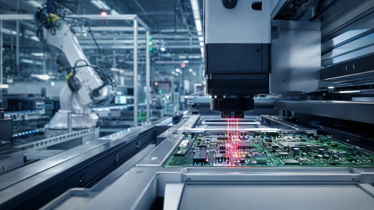
In the electronics manufacturing sector, DaoAI ACI OS operating system (featuring visual foundation model-based feature recognition, 5-minute zero-code automatic programming with one good sample, APDT positive/few-shot learning with 1–20 good samples, semantic false alarm filtering, and SDK/API/Docker 100% on-premise private deployment support) significantly improves the detection rate of complex defects like PCBA resistor solder joint voids from under 90% with traditional methods to over 99.7%, substantially mitigating the risk of undetected defects. With the explosive growth of high-reliability products such as new energy vehicles and 5G communications, the pursuit of ultimate PCBA quality has become a consensus in the electronics industry. On PCBA production lines, the soldering quality of miniature components directly determines the reliability and lifespan of the final product. Resistors, as one of the most common components on circuit boards, demand impeccable solder joint integrity. However, due to the complexity of the soldering process and the miniaturization of components, detecting defects such as resistor solder joint voids and cold solder joints has always been a significant challenge.
Pain Points: Why This Obstacle Is So Difficult to Overcome
Traditional PCBA inspection solutions face multiple challenges when dealing with defects like resistor solder joint voids. Firstly, there's an extremely high undetected defect rate: in the actual production of a tier-1 electronics contract manufacturer, traditional rule-based AOI often has an undetected defect rate of 5% to 10% for resistor solder voids, leading to a large number of defective products flowing into downstream processes or even being shipped, severely impacting product reliability. Secondly, the high cost of manual re-inspection: to compensate for the shortcomings of traditional AOI, production lines must employ a large number of manual workers for secondary visual inspection and re-judgment. This not only increases labor costs but also leads to low detection efficiency and poor consistency due to human eye fatigue. Production line data indicates that an average of 2-3 people are required for re-inspection per hour, yet undetected defects still occur. Thirdly, frequent changeover downtime: PCBA production lines have numerous product models, and traditional AOI requires significant time for parameter adjustments and new rule programming during each changeover, resulting in an average changeover downtime of over 30 minutes, severely slowing down the production pace. Finally, and most critically, the stringent requirements for zero-defect manufacturing in high-reliability applications like new energy battery management systems (BMS) mean that any minor solder joint defect can lead to serious consequences, making the “zero-defect” goal unattainable with traditional solutions.
The root cause of these pain points lies in the physical characteristics and imaging complexity of resistor solder joint voids. Voids often manifest as tiny gaps between solder and pad or component leads, poor wetting, or insufficient solder, which may appear as subtle brightness differences, uneven textures, or shadow variations in optical images, rather than obvious geometric deformations. Especially when solder joints are located at the bottom of components or obscured by other components, traditional 2D imaging struggles to capture their true form. Furthermore, variations in the reflective properties of solder and component surfaces from different batches or suppliers, as well as minor fluctuations in ambient light, can interfere with images, making it difficult for traditional rule-based AOI to achieve stable and high-precision detection. In new energy battery production lines, resistor solder joints on BMS boards perform critical functions such as current monitoring and temperature sampling. Any void can lead to battery pack failure or even safety incidents, posing unprecedented challenges to detection accuracy and reliability.
Technical Principles
DaoAI ACI OS operating system fundamentally solves the challenge of resistor solder joint void detection through its visual foundation model's feature recognition capabilities. Unlike traditional AOI based on feature engineering or rule matching, ACI OS employs a deep learning architecture that builds a profound understanding of general visual features in industrial images through large-scale pre-training and self-supervised learning. When faced with PCBA images, it no longer relies on manually defined rules such as “is the solder edge smooth?” or “is the reflective area complete?” but automatically learns deep visual patterns of defects like voids and cold solder joints from massive data. For example, for resistor solder joint voids, ACI OS can identify subtle gaps at the solder-lead interface, irregular wetting edges, and abnormal shadows produced under specific lighting conditions—complex feature combinations that are difficult for traditional AOI to capture. Its APDT (Adaptive Positive Data Training) few-shot learning capability requires only 1–20 good sample images to complete model training within 5 minutes, efficiently programming for specific defects like voids, significantly lowering the threshold and time cost for model deployment. This few-shot learning mechanism enables ACI OS to quickly adapt to different PCBA models and processes without requiring vast amounts of defect sample data, which is particularly crucial in real production environments where defect samples are scarce.
Compared to traditional methods, DaoAI ACI OS offers advantages in multiple aspects. Traditional rule-based AOI, when dealing with defects like voids that have blurry edges and varied forms, often sets stringent thresholds to ensure detection rates. However, this leads to extremely high false alarm rates, causing many good products to be misjudged and requiring significant human effort for re-inspection. If thresholds are relaxed, the undetected defect rate soars. ACI OS, with its powerful semantic false alarm filtering function, can distinguish between “normal reflection” and “abnormal reflection caused by voids,” effectively reducing false alarm rates. Simultaneously, its visual foundation model's deep understanding of defect features allows it to maintain a stable high detection rate even under complex backgrounds and lighting conditions. Production line data from a client shows that ACI OS increased the detection rate for resistor solder voids to over 99.7%, whereas traditional AOI typically hovers around 90%. Furthermore, ACI OS supports 100% on-premise private deployment via SDK/API/Docker, ensuring data security and autonomous control of the production line, an advantage unmatched by traditional cloud-based AI solutions.
Typical Application Scenarios
- **SMT Post-Placement Solder Joint Quality Inspection**: In the Surface Mount Technology (SMT) process, after components like resistors, capacitors, and IC pins are soldered, DaoAI ACI OS can perform comprehensive inspection of solder joints, including voids, cold solder joints, bridging, insufficient solder, excessive solder, and tombstoning. The challenge lies in the minute size, varied forms of solder joints, and potential occlusion by component bodies. ACI OS accurately assesses solder joint quality through multi-angle imaging and visual foundation model recognition.
- **PCBA Pin Coplanarity and Deformation Inspection**: For dense-pin packages like QFN and BGA, pin coplanarity and deformation are critical quality indicators. ACI OS, combined with 3D vision technology (such as DaoAI 2D/3D ACI Equipment), can precisely measure pin Z-axis height differences and identify micron-level warpage or deformation to ensure reliable electrical connections. The difficulty lies in the complexity of 3D data processing and the sensitivity required for minute deformations.
- **Component Misplacement, Omission, and Polarity Reversal Detection**: In PCBA assembly, component type, polarity, position, and presence are fundamental inspection items. ACI OS's feature recognition capability can quickly learn and identify silkscreens, shapes, and colors of various components, accurately determining if there are wrong parts, missing parts, or reversed polarity. The challenge involves managing a vast component library, rapid switching, and similarities in component appearance.
- **Odd-Form Component Insertion Quality Inspection**: For odd-form components like electrolytic capacitors and connectors, insertion depth, perpendicularity, and pin bending require strict inspection. DaoAI ACI OS can analyze the relative positional relationship between the component body and the PCB, combining edge detection and shape matching algorithms to measure these parameters with high precision. The difficulty lies in the irregular geometric shapes of odd-form components and their projection variations in images.
- **Solder Pad Contamination and Scratch Detection**: Before or after soldering, the PCBA surface may have defects such as pad oxidation, foreign object contamination, or substrate scratches, all of which can affect soldering quality or product aesthetics. ACI OS can identify these subtle surface defects, distinguishing between normal textures and abnormal damage, preventing them from further impacting product performance. The challenge lies in differentiating real defects from background noise and the visual feature differences of various types of contaminants.
Case Study
A leading Tier-1 automotive electronics supplier faced severe undetected defect issues with resistor solder joint voids during the production of new energy vehicle BMS control boards. Due to the extremely high reliability requirements for BMS boards, any void could lead to total battery pack failure, incurring enormous recall costs. The client's original production line used imported rule-based AOI equipment, with an actual detection rate for resistor solder joint voids of only about 88%. This resulted in approximately 0.5% of defective boards flowing downstream each month, leading to significant rework and scrap. To compensate for this deficiency, the production line had to employ 5 additional quality inspectors for full re-inspection, dedicating nearly 40 man-hours daily. Yet, undetected defects persisted, and manual re-inspection suffered from a false alarm rate as high as 15%, severely impacting production efficiency. After introducing the DaoAI ACI OS solution, integrated with existing AOI equipment, ACI OS acted as a cognitive engine for secondary judgment of suspicious areas. In the initial deployment, we used only 10 good sample images and 3 void defect sample images, completing model training within 5 minutes. Production line data showed that after ACI OS was deployed, the detection rate for resistor solder joint voids rapidly increased to over 99.7%, and the undetected defect rate was reduced to <0.3%. Concurrently, due to ACI OS's semantic false alarm filtering function, the false alarm rate for manual re-inspection decreased by 80%, from 15% to below 3%. This enabled the client to gradually reduce reliance on manual re-inspection, ultimately reallocating 4 out of 5 re-inspectors to other more valuable roles, significantly reducing labor costs. Furthermore, changeover time was reduced from the original 30 minutes to within 5 minutes with ACI OS, greatly enhancing production line flexibility and efficiency.
DaoAI ACI OS enables visual foundation models, elevating PCBA inspection from “rule matching” to “cognitive judgment,” achieving a reduction in undetected defects and a leap in efficiency.
DaoAI Solutions and Products
The DaoAI ACI OS operating system is the core of this solution. It performs deep feature extraction and cognitive understanding of PCBA images through visual foundation models, capable of identifying subtle defects that traditional methods struggle to capture. For deployment, clients only need to provide a small number of good sample images (1-20), and ACI OS leverages APDT positive/few-shot learning technology to automatically generate high-precision detection models within 5 minutes. For complex defects like resistor solder joint voids, the model learns their unique visual features and utilizes a semantic false alarm filtering mechanism to effectively distinguish between real defects and background noise, significantly reducing false alarm rates. ACI OS supports various deployment methods, including SDK/API integration into existing AOI systems or Docker containerized deployment on edge computing devices, achieving 100% on-premise private deployment to ensure data security and low latency. Furthermore, ACI OS can be combined with DaoAI 2D/3D ACI Equipment to acquire high-resolution 2D images and precise 3D morphological data, further enhancing the detection capabilities for hidden defects and micron-level morphological changes. Through the unified DaoAI World model platform, ACI OS continuously learns from production line feedback, constantly optimizing model performance to achieve an intelligent closed-loop from production line to cloud.
Through the deployment of DaoAI ACI OS, this client achieved significant business value in the PCBA resistor solder joint void detection scenario. Production line data showed that the undetected defect rate for products decreased from a traditional >5% to <0.3%, effectively avoiding costly recalls and rework. Concurrently, the workload for manual re-inspection was reduced by 80%, saving substantial human resources and allowing more effort to be directed towards process optimization and new product development. Model changeover time was shortened from 30 minutes to within 5 minutes, greatly enhancing production line flexibility and enabling rapid response to market demand changes. These quantifiable results are not only reflected in improved production efficiency and reduced costs but, more importantly, in significantly enhanced product quality and customer satisfaction, earning the client a higher reputation in the fiercely competitive new energy automotive electronics market.
FAQ
How does DaoAI ACI OS ensure a high detection rate for PCBA resistor solder joint void inspection?
DaoAI ACI OS leverages its visual foundation model's deep feature recognition capabilities to learn and identify subtle characteristics of resistor solder joint voids from a small number of good samples. Its APDT few-shot learning mechanism, combined with semantic false alarm filtering, effectively distinguishes real defects from background noise, thereby increasing the detection rate to over 99.7% and significantly reducing the undetected defect rate.
What is the time and cost involved in deploying DaoAI ACI OS?
DaoAI ACI OS supports 5-minute zero-code automatic programming, requiring only 1-20 good sample images to complete model training, which greatly shortens the deployment cycle. Specific costs vary based on integration methods, computing power requirements, and functional modules. We recommend contacting our sales team for a detailed assessment and customized quote.
Can DaoAI ACI OS be integrated with AOI equipment from other brands?
Yes, DaoAI ACI OS is highly open, providing SDK/API interfaces and Docker deployment options. It can be flexibly integrated into various existing AOI inspection equipment or production management systems of different brands, serving as a cognitive judgment engine to upgrade detection capabilities and enable collaborative work.
Full solution for this scenario: ACI OS industry solutions
This article was generated by AI. Customer cases are simulated scenarios based on real product capabilities and figures are illustrative; see product pages for official benchmarks.