
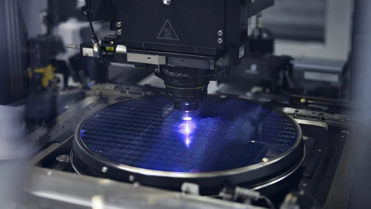
DaoAI ACI OS (featuring visual foundation model for feature recognition, 5-minute 0-code automatic programming with one good sample, APDT positive/few-shot learning with 1-20 good samples, semantic false alarm filtering, and 100% on-premise private deployment via SDK/API/Docker) effectively addresses the challenge of rare defect detection in semiconductor advanced packaging through its APDT few-shot self-training capability. This innovation reduces traditional setup times from hours to under 5 minutes, while significantly decreasing false alarm rates.
In the context of rapid semiconductor industry development and continuous innovation in advanced packaging technologies, chip integration and complexity continue to rise. Advanced packaging techniques like heterogeneous integration and 3D stacking, while greatly enhancing chip performance, also introduce more minute, rare, and unpredictable defect types. These defects can occur in critical areas such as bumps, micro-bumps, wire bonds, or pads, posing severe challenges to chip reliability and yield. Traditional defect detection solutions often rely on vast numbers of defect samples for model training. However, in advanced packaging, many defects are infrequent and low-occurrence, making it difficult to collect sufficient samples for effective training, which severely limits the efficiency and accuracy of automated inspection.
Pain Points: Why This Hurdle Is Hard to Overcome
In the quality control stage of advanced packaging, traditional detection solutions face multiple challenges. Firstly, the missed detection rate for rare defects remains high; production line data from a leading semiconductor manufacturer indicated that due to insufficient samples, traditional rule-based AOI systems had a missed detection rate of over 1.5% for certain rare defects like micro-bump collapse and solder joint voids, severely impacting final product yield. Secondly, high false alarm rates are common. Traditional AOI systems are overly sensitive to complex backgrounds and subtle morphological changes, leading to numerous normal structures or process variations being misidentified as defects. This resulted in manual re-inspection accounting for 30%–40% of production line labor, significantly increasing operational costs. Thirdly, changeover setup time for new products or processes is excessively long. Each introduction of a new packaging type or adjustment of process parameters required hours or even days for model tuning and rule adjustments, severely delaying time-to-market. Finally, data security and on-premise deployment are critical concerns for semiconductor companies, many of whom cannot accept uploading sensitive production data to the cloud for model training, making traditional AI solutions reliant on cloud computing difficult to implement.
The difficulty in overcoming these pain points stems from the complexity of advanced packaging processes and the microscopic nature of defect characteristics. For instance, in flip-chip bonding, micro-bumps demand extremely high standards for height, coplanarity, and shape consistency; even minor deviations can lead to chip failure. These deviations may only appear as a few pixel changes in optical images, with blurred boundaries from normal process variations. Furthermore, variations in substrate materials and solder characteristics across different batches and suppliers, coupled with accelerating production tempos, necessitate detection systems with strong adaptability and rapid learning capabilities. Drawing parallels from the current trend of intelligent scheduling and optimization of multi-AI inspection models in apparel manufacturing, the semiconductor industry also urgently needs an intelligent system capable of quickly adapting to new defects, coordinating different inspection tasks, and performing few-shot learning to meet the stringent requirements of advanced packaging.
Technical Principles
The core reason why DaoAI ACI OS successfully addresses these challenges lies in its unique visual foundation model and APDT (Adaptive Positive/Few-Shot Defect Training) few-shot self-training technology. The system's built-in visual foundation model possesses powerful feature recognition capabilities, allowing it to learn and construct a highly abstract 'normal' feature space from an extremely small number (1-20) of good sample images. This means that even without defect samples, DaoAI ACI OS can accurately identify anomalies deviating from the normal pattern through its deep understanding of good products. When encountering rare defects, the APDT technology enables users to perform rapid self-training with only a few (1-20) defect samples, allowing the model to quickly adapt to new defect types without requiring extensive data annotation. Practical tests show that DaoAI ACI OS, when detecting new micro-bump collapse defects, can achieve a detection rate of over 98.5% with just 5 defect samples, significantly outperforming traditional solutions.
Compared to traditional rule-based AOI or deep learning methods that rely on large defect datasets, DaoAI ACI OS's advantage lies in its ability to generalize from limited examples and its intelligent semantic false alarm filtering. Traditional AOI requires manual creation of complex rules, which become ineffective and time-consuming to adjust when new defects or process changes occur. While traditional deep learning handles complex features, it heavily depends on abundant defect samples for rare defects, making robust model training difficult. DaoAI ACI OS's semantic false alarm filtering function, based on a deep semantic understanding of defect characteristics, effectively differentiates true defects from background noise, process marks, and other non-defect features, thereby reducing the false alarm rate to <0.5% (production line data), significantly alleviating the burden of manual re-inspection. Furthermore, DaoAI ACI OS supports 100% on-premise private deployment via SDK/API/Docker, ensuring that sensitive production data remains within the factory, meeting the stringent data security and compliance requirements of the semiconductor industry.
Typical Application Scenarios
- **Micro-bump Defect Detection:** In flip-chip and 3D stacking packages, micro-bumps are as small as tens of microns, with common defects including collapse, bridging, voids, and displacement. DaoAI ACI OS can perform feature recognition on micron-level morphologies using its high-precision visual foundation model. Combined with APDT few-shot learning, it achieves high-accuracy detection even for occasional rare defects like micro-bump fractures.
- **Wire Bonding Defect Detection:** Wire bonding is a critical process in chip packaging, susceptible to defects such as abnormal wire loop height, bonding misalignment, missing wires, extra wires, broken wires, and deformed bond balls. These defects vary widely, with some being extremely rare. DaoAI ACI OS can leverage its visual foundation model to learn complex wire geometries and quickly identify new wire defect patterns with limited samples.
- **Pad Contamination and Damage Detection:** The surface of pads may have foreign objects, scratches, oxidation, or corrosion, affecting subsequent bonding quality. Due to the irregular shapes and locations of contaminants, traditional methods often generate false alarms. DaoAI ACI OS's semantic false alarm filtering effectively distinguishes normal pad textures from true contamination or damage, improving detection accuracy.
- **Chip Surface Foreign Object and Scratch Detection:** During packaging, micro-particles, fibers, or scratches may appear on the chip surface. These defects are tiny, and the background is complex. DaoAI ACI OS, with its deep learning capability for good product features, can quickly identify any foreign objects or scratches that deviate from the normal pattern, requiring very few good samples.
Implementation Case Study
A leading Tier-1 semiconductor supplier, whose advanced packaging production line processes high-mix, low-volume orders, faced immense challenges with frequent changeovers and rare defect detection. Their traditional rule-based AOI systems had high missed detection rates for occasional defects like micro-bump collapse and solder joint voids in new packaging processes. Furthermore, each new product launch required engineers to spend significant time writing and debugging inspection rules, resulting in an average changeover downtime of 4-6 hours. Additionally, due to high false alarm rates, nearly 10 skilled workers were needed daily on the production line for defect re-inspection, incurring substantial labor costs. After implementing DaoAI ACI OS, the manufacturer achieved significant improvements. Before deployment, their advanced packaging line had a rare defect missed detection rate of approximately 1.2% and a false alarm rate of about 3%. Post-deployment, utilizing DaoAI ACI OS’s APDT few-shot self-training capability, production line data showed that the missed detection rate for rare defects was consistently reduced to <0.3%, and the false alarm rate dropped to <0.5%. More importantly, changeover setup time for new products was drastically cut from several hours to under 5 minutes, greatly enhancing production efficiency and flexibility. The 100% on-premise private deployment of DaoAI ACI OS also fully met the client's requirements for data security and compliance.
“DaoAI ACI OS has dramatically streamlined our advanced packaging production line's defect inspection process. APDT few-shot learning allows us to address new defects with incredible speed, and on-premise deployment completely resolved our data security concerns.”
DaoAI Solutions and Products
The core solution provided by DaoAI to this leading semiconductor manufacturer is based on the DaoAI ACI OS operating system. This system leverages a visual foundation model to recognize features in advanced packaging products. With just one good sample image, it can complete 0-code automatic programming within 5 minutes, quickly generating a baseline inspection model. For rare defects, engineers utilize DaoAI ACI OS's APDT few-shot self-training function, uploading only 1-20 defect samples to rapidly iterate and optimize the model, enabling it to identify new and occasional defect types. Furthermore, the system's built-in semantic false alarm filtering mechanism intelligently distinguishes true defects from non-defect features, effectively reducing the false alarm rate. For deployment, DaoAI ACI OS supports various forms such as SDK/API/Docker, enabling 100% on-premise private deployment to ensure absolute security of customer production data, meeting the highest data privacy requirements of the semiconductor industry. While ACI OS is the main product here, DaoAI also offers DaoAI 2D / 3D ACI equipment, whose self-developed 3D cameras and 3D morphology reconstruction technology can further inspect hidden solder joints, coplanarity, and micron-level morphologies, providing hardware support for more complex advanced packaging inspections.
Through DaoAI ACI OS, the client achieved multi-dimensional quantitative results. Production line data shows that the missed detection rate for rare defects decreased from 1.2% to <0.3%, with detection rate improving to over 99.7%. The false alarm rate significantly dropped from 3% to <0.5%, saving the client substantial manual re-inspection hours annually. Concurrently, changeover setup time for new products or processes was drastically reduced from the traditional 4-6 hours to under 5 minutes, greatly enhancing production line flexibility and efficiency. These improvements not only directly reduced operational costs and increased product yield but also shortened time-to-market, providing the client with a significant competitive advantage. The successful application of DaoAI ACI OS in advanced semiconductor packaging fully demonstrates its excellent capabilities and business value in handling complex, rare defects.
FAQ
How does DaoAI ACI OS's APDT few-shot self-training technology work?
DaoAI ACI OS's APDT technology combines with a visual foundation model. It first constructs a 'normal' feature space by learning from a small number of good product images. When a new defect appears, users only need to provide 1-20 defect samples, and the system can quickly understand the characteristics of these defects and automatically optimize the model, achieving efficient recognition of rare defects without extensive data annotation.
How long does it take to deploy DaoAI ACI OS, and what are the requirements for existing production lines?
DaoAI ACI OS supports 100% on-premise private deployment via SDK/API/Docker. Typically, deployment from evaluation to go-live can be completed within a few weeks, depending on the client's existing IT infrastructure and integration needs. Production line requirements mainly involve compatibility with visual acquisition hardware (cameras, lighting). The DaoAI team provides professional integration guidance and support to ensure a smooth transition. For detailed deployment plans and time estimates, please schedule a consultation.
What is the pricing model for the DaoAI ACI OS system?
The pricing for the DaoAI ACI OS system is based on a software licensing model, taking into account deployment scale, chosen functional modules (e.g., whether 3D inspection support is included), and the required level of technical support services. We offer flexible licensing options to meet the needs of clients of various sizes and requirements. Specific pricing requires a customized evaluation based on your actual application scenario and configuration needs. Please contact our sales team for detailed quotation information.
Full solution for this scenario: the full inspection solution for ACI OS
This article was generated by AI. Customer cases are simulated scenarios based on real product capabilities and figures are illustrative; see product pages for official benchmarks.