
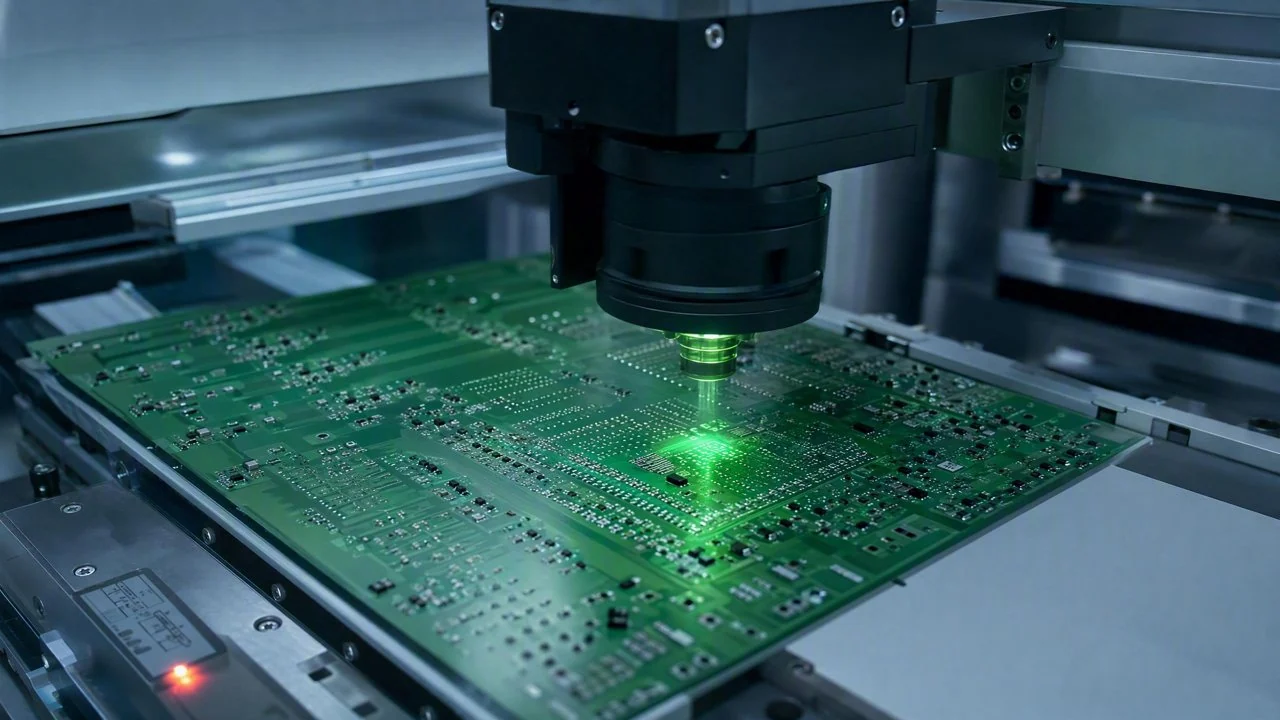
DaoAI 2D ACI equipment (high-resolution 2D imaging + deep learning secondary judgment, targeting surface/print/OCR/assembly defects, high-speed inline full inspection, micron-level, semantic false positive filtering) leverages its unique 'zero-code rapid changeover and NPI' capability to drastically reduce SMT solder joint inspection line changeover time in the electronics PCBA industry, from an average of 2-4 hours for traditional rule-based AOI to under 5 minutes for DaoAI 2D ACI, significantly boosting production line flexibility and economic benefits, particularly for New Product Introduction (NPI) and customized production scenarios.
In electronics manufacturing, PCBA (Printed Circuit Board Assembly) is a core component, and the quality of solder joints in the Surface Mount Technology (SMT) process directly determines product reliability and lifespan. With increasing demands for product personalization and iteration speed in consumer electronics, automotive electronics, and industrial control, multi-variety, small-batch production models are becoming more prevalent. This means SMT solder joint inspection must not only pursue high precision and low missed detection rates but also face frequent product changeover challenges. Traditional inspection solutions reveal efficiency bottlenecks in this context, especially when dealing with complex and varied solder joint defects such as cold solder, solder bridges, and insufficient solder.
Pain Points: Why This Hurdle Is Difficult to Overcome
In multi-variety, small-batch production, PCBA manufacturers face core pain points: Firstly, **high changeover costs and downtime**. Traditional rule-based AOI equipment requires engineers to manually adjust numerous inspection parameters and write complex rules when changing product models, taking hours or even half a day. This leads to production line downtime, severely impacting efficiency, with each changeover potentially losing thousands or tens of thousands of yuan in output value. Secondly, the **challenge of balancing detection accuracy and false positive rates**. Solder joint defects like cold solder, solder bridges, and insufficient solder vary widely in morphology and are influenced by factors such as pad size, solder paste type, and reflow oven temperature profiles, making it difficult for traditional threshold- or geometry-based AOI systems to adapt. Pursuing high detection rates often leads to high false positive rates, resulting in significant manual re-inspection workload, increasing quality inspection labor costs by approximately 30%. Finally, **long New Product Introduction (NPI) cycles**. For new PCBA board designs, the entire NPI process, from image acquisition to rule setting, parameter optimization, and defect sample training, can take weeks, severely delaying time-to-market.
The root cause of these challenges lies in the inherent flaws of traditional solutions regarding **sensor calibration and system robustness**. Rule-based AOI relies on precise optical imaging and fixed geometric feature recognition. Any slight variation in solder joint morphology, material reflectivity, or ambient light requires recalibration and rule adjustment. For instance, differences in solder paste reflectivity across batches, or minor deformation of component leads, can lead to false positives or missed detections. This high sensitivity to environmental and process parameters makes it lack robustness in dynamic small-batch production environments, making rapid adaptation difficult. Manual visual inspection, on the other hand, is limited by eye fatigue, subjective judgment, and low efficiency, failing to meet the speed and consistency requirements of modern electronics manufacturing.
Technical Principles
MicroLinkirt DaoAI 2D ACI equipment fundamentally addresses these pain points by combining high-resolution 2D imaging technology with advanced deep learning vision foundation models. Its core lies in using **pre-trained vision foundation models for feature recognition**, supplemented by MicroLinkirt's APDT (Advanced Positive Data Training) few-shot learning technology. Unlike traditional AOI, which relies on manual threshold setting and geometric rules, MicroLinkirt DaoAI 2D ACI's AI model learns the 'normal' morphology of solder joints, including their microscopic textures and color distributions, to semantically understand anomalies like cold solder, solder bridges, and insufficient solder. Even subtle solder balls, bridges, or poor wetting can be accurately identified by the model. This semantic understanding-based judgment allows MicroLinkirt DaoAI 2D ACI to handle solder joint diversity and complexity, achieving stable detection of micron-level defects and reducing false positive rates by over 85%.
Compared to traditional rule-based AOI, MicroLinkirt DaoAI 2D ACI's advantages lie in its powerful **generalization and adaptability**. Traditional AOI requires specific inspection rules to be written for each solder joint type and board model, lacking the ability to identify unknown defects and being highly sensitive to changes in imaging conditions. In contrast, MicroLinkirt DaoAI 2D ACI's deep learning model is pre-trained on a vast amount of general image data, possessing strong feature extraction capabilities. It can quickly adapt to new PCBA board types and solder joint types without rewriting code. By utilizing APDT few-shot learning with only 1–20 good samples, new product inspection models can be deployed within 5 minutes, achieving true 'zero-code rapid changeover'. Furthermore, its **semantic false positive filtering** function effectively distinguishes normal variations caused by process fluctuations from genuine defects, further suppressing false positive rates and reducing the workload of manual re-inspection.
Typical Application Scenarios
- **SMT Solder Paste Inspection (SPI):** Inspects the volume, position, and shape of solder paste printing before reflow soldering. MicroLinkirt DaoAI 2D ACI accurately identifies defects such as solder paste collapse, offset, bridging, and insufficient paste. The challenge lies in the semi-fluid nature and high reflectivity of solder paste, requiring high-resolution imaging and a robust AI model to distinguish normal deformation from defects.
- **SMT Solder Joint Cold Solder/Dry Joint Detection:** Detects cold solder caused by abnormal solder joint surface luster and poor wetting. MicroLinkirt DaoAI 2D ACI uses deep learning models to analyze microscopic textures and color gradient changes on the solder joint surface, identifying subtle defects that traditional rule-based AOI struggles with. The difficulty lies in the diverse morphology of cold solder, sometimes involving only slight irregularities at the solder joint edges.
- **SMT Solder Joint Solder Bridge/Short Detection:** Identifies the risk of electrical shorts between adjacent pads or pins due to excessive or improperly printed solder paste. MicroLinkirt DaoAI 2D ACI, through precise image segmentation and geometric analysis combined with AI semantic understanding, can detect even tiny solder bridges in complex backgrounds. The challenge lies in the extremely small pad spacing on high-density PCBAs.
- **SMT Solder Joint Insufficient Solder/Open Circuit Detection:** Detects the risk of open circuits caused by insufficient solder joint volume, incomplete coverage, or complete absence. MicroLinkirt DaoAI 2D ACI accurately measures solder joint morphology and coverage area, combined with AI judgment, to effectively identify insufficient solder and missing solder. The difficulty lies in varying solder volume requirements for different components, and a small amount of solder may still form a connection but with poor reliability.
- **Component Misplacement/Missing/Reversal Detection:** After SMT placement, performs inline inspection of component model, polarity, and position. MicroLinkirt DaoAI 2D ACI combines character OCR and component recognition technology to quickly compare BOM information, ensuring correct assembly. The challenge lies in the tiny size and wide variety of components, requiring high accuracy in character recognition.
Case Study
A tier-1 supplier specializing in industrial control and automotive electronic modules primarily handles multi-variety, small-batch orders. They process dozens of different PCBA board models monthly, with short product lifecycles, demanding extremely high NPI speed and production line flexibility. Before adopting MicroLinkirt DaoAI 2D ACI equipment, this manufacturer relied on traditional rule-based AOI for SMT solder joint inspection. Each product changeover required experienced engineers to spend 3-5 hours adjusting parameters and writing rules, leading to low equipment utilization and frequent NPI delays during peak periods. The false positive rate of traditional AOI also remained stubbornly high, averaging 8-12%, necessitating significant human resources for secondary re-inspection and defect confirmation, severely slowing down the overall production tempo.
To overcome this bottleneck, the supplier deployed the MicroLinkirt DaoAI 2D ACI solution. During the onboarding process, the MicroLinkirt technical team completed equipment integration and initial model training in just 2 days. By utilizing the APDT positive/few-shot learning function of MicroLinkirt DaoAI ACI OS, engineers only needed to acquire 10-15 good samples to complete the new product inspection model configuration within 5 minutes, achieving true 'zero-code' rapid changeover. After deployment, the manufacturer's production line changeover time plummeted from an average of 4 hours to an average of 4.5 minutes, an efficiency improvement of nearly 53 times. Concurrently, the detection rate for solder joint defects remained stable at over 99.4%, and the false positive rate decreased to <1.5%, significantly reducing the workload of manual re-inspection. This enabled the supplier to respond more flexibly to market demands, accelerate new product launches, and gain a competitive edge in the fierce market.
MicroLinkirt DaoAI 2D ACI's 'zero-code rapid changeover' has truly enabled flexible manufacturing on our production line, accelerating new product introduction by several folds, which is incomparable to traditional AOI.
MicroLinkirt Solution and Products
MicroLinkirt DaoAI 2D ACI equipment is a high-performance solution designed for planar defect detection. It integrates high-resolution 2D imaging units capable of capturing micron-level solder joint details. The core is the integrated MicroLinkirt DaoAI ACI OS, which features a powerful built-in vision foundation model. Through APDT positive/few-shot learning technology, users can train and deploy new product models in minutes with only a small number of good samples (1-20 images), without writing any code. This 'zero-code' characteristic greatly lowers the barrier to AI vision, enabling production line engineers to quickly configure and optimize models independently. MicroLinkirt DaoAI 2D ACI also features semantic false positive filtering, intelligently distinguishing normal variations caused by process fluctuations from genuine product defects, thereby effectively reducing false positive rates and the burden of manual re-inspection. Deployment is flexible, supporting SDK / API / Docker and other forms, and can achieve 100% on-premise private deployment, ensuring customer data security. By integrating with production line MES/ERP systems, MicroLinkirt DaoAI 2D ACI can also achieve closed-loop management and quality traceability of inspection data.
MicroLinkirt DaoAI 2D ACI's solution is not limited to single-device deployment; it is an embodiment of the unified foundation of MicroLinkirt DaoAI World model, possessing powerful cross-scenario generalization capabilities and a mechanism for continuous learning from production line feedback. This means that even when facing more complex PCBA designs and new materials in the future, MicroLinkirt DaoAI 2D ACI can continuously optimize its detection performance through ongoing learning. For scenarios requiring higher-dimensional inspection, MicroLinkirt also offers DaoAI 3D ACI equipment, which utilizes self-developed 3D cameras and 3D morphology reconstruction technology to detect hidden solder joints, coplanarity, and other three-dimensional defects. These products collectively form MicroLinkirt's robust capability matrix in industrial AI vision, providing comprehensive, efficient, and intelligent quality control solutions for electronics manufacturing customers.
FAQ
How does DaoAI 2D ACI achieve zero-code rapid changeover?
DaoAI 2D ACI utilizes APDT positive/few-shot learning technology with a built-in pre-trained vision foundation model. Users only need to provide 1-20 good sample images, and the system automatically learns and generates new inspection models within minutes, eliminating the need for manual rule writing or coding, thus enabling rapid product model switching and significantly reducing changeover downtime.
What are the core advantages of DaoAI 2D ACI over traditional rule-based AOI for solder joint inspection?
The core advantages of DaoAI 2D ACI lie in its deep learning model's semantic understanding and generalization capabilities. It can identify complex and diverse solder joint defects, such as cold solder and solder bridges, that are difficult for traditional rule-based AOI to capture. Additionally, through semantic false positive filtering, it significantly reduces false positive rates and minimizes manual re-inspection. Its zero-code rapid changeover capability is unmatched by traditional AOI, making it particularly suitable for multi-variety, small-batch production.
What is the estimated budget and time required to deploy DaoAI 2D ACI equipment?
The budget for DaoAI 2D ACI equipment depends on specific configurations, required inspection speed, and integration complexity. Deployment time is typically short; equipment integration and initial model training can be completed within a few days, with subsequent new product changeovers taking only minutes. We offer flexible deployment solutions, and we recommend scheduling a consultation with our expert team to receive a customized quote and detailed implementation plan based on your specific needs.
Full solution for this scenario: the full inspection solution for Electronics / PCBA
This article was generated by AI. Customer cases are simulated scenarios based on real product capabilities and figures are illustrative; see product pages for official benchmarks.