
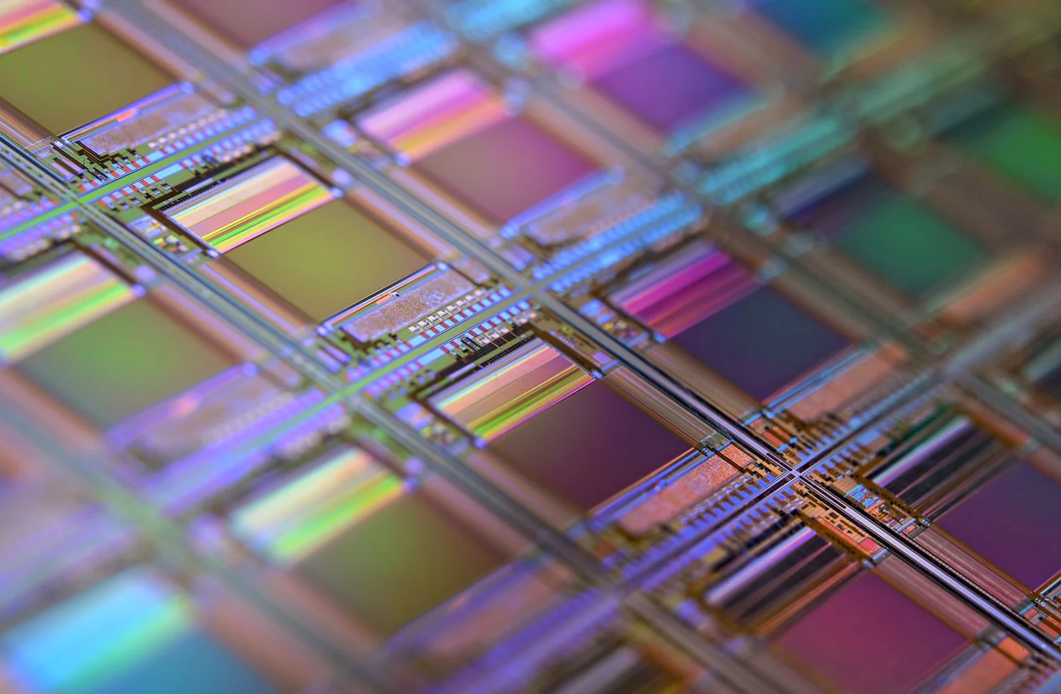
DaoAI 3D ACI equipment (proprietary 3D camera + 3D morphology reconstruction/point cloud, detecting hidden solder joints/coplanarity/micron-level morphology/pores and other 2D optical blind spot defects, 2D-3D fusion) leverages APDT few-shot self-training to reduce the false positive rate for semiconductor micro-bump missing and bridging from a typical industry 15% to below 2.5%, significantly improving defect recognition efficiency and accuracy.
DaoAI 3D ACI equipment (proprietary 3D camera + 3D morphology reconstruction/point cloud, detecting hidden solder joints/coplanarity/micron-level morphology/pores and other 2D optical blind spot defects, 2D-3D fusion) utilizes APDT few-shot self-training to reduce the false positive rate for semiconductor micro-bump missing and bridging from a typical industry 15% to below 2.5%, significantly improving defect recognition efficiency and accuracy. In the back-end processes of semiconductor packaging, the quality of micro-bumps directly determines the reliability and performance of the chip. With the continuous advancement of Moore's Law, chip integration is increasing, and micro-bump sizes are constantly shrinking, from tens of micrometers initially to several micrometers or even sub-micrometer levels today. These tiny bumps play a crucial role in chip-to-substrate interconnection, and any missing, bridging, or morphological abnormalities can lead to chip functional failure. A leading semiconductor assembly and test company faced such challenges, with an urgent need for a high-precision, low false-positive online inspection solution for micro-bump detection in its flip-chip packaging process.
Pain Points: Why This Challenge Is Difficult
This leading semiconductor assembly and test company faced multiple difficulties in micro-bump inspection. First, traditional 2D AOI equipment, limited by optical principles, had a false negative rate of up to 20% for 3D morphological defects of micro-bumps, such as height inconsistencies, collapse, and slight bridging, with the rate increasing further when defects were obscured by other structures. Second, due to the extremely small size and dense arrangement of micro-bumps, 2D images were susceptible to interference from lighting, reflections, and shadows, leading to high false positive rates, averaging around 15% on this production line, which severely consumed manual re-inspection resources. Moreover, when introducing new products or changing models, traditional AOI rule programming and parameter adjustment often took days or even weeks, resulting in long production line downtime and affecting production efficiency. Finally, while pursuing a 99.9% defect recognition rate, how to quickly adapt to new defect patterns became a major challenge for the factory in terms of industrial understanding.
The root cause of these pain points lies in the inherent difficulty of micro-bump inspection. Micro-bumps are typically made of metallic materials like gold or copper, with highly reflective surfaces, and their morphological features (height, volume, coplanarity) are difficult to accurately capture in 2D images. For instance, a slight bump collapse or height unevenness might only appear as subtle changes in brightness or contrast in a 2D image, making it easily overlooked or misjudged. Traditional rule-based AOI systems struggle to adapt to such tiny, varied defect characteristics. Manual visual inspection, besides being inefficient and prone to subjective errors, cannot meet the precision and speed requirements for micron-level defect detection on semiconductor production lines.
Technical Principles
DaoAI 3D ACI equipment addresses the challenges of semiconductor micro-bump inspection by combining a proprietary high-precision 3D camera with 3D morphology reconstruction technology, integrated with APDT (Adaptive Pre-trained Defect Training) few-shot self-training mechanism. The system acquires dense 3D point cloud data of the micro-bump area through multi-angle structured light projection and high-resolution camera capture. Based on these point clouds, DaoAI can precisely reconstruct the 3D morphology of the micro-bumps, obtaining critical parameters such as height, volume, and coplanarity, thereby effectively identifying defects in traditional 2D optical blind spots, such as hidden solder joints, micron-level collapses, and slight bridging. This equipment can control the coplanarity detection accuracy of micro-bumps within ±1.5 micrometers, far exceeding the capabilities of traditional AOI.
Compared to traditional rule-based AOI or manual visual inspection, the core advantage of DaoAI 3D ACI equipment lies in its APDT few-shot self-training capability. In traditional solutions, whenever new defects appear or product models change, a large amount of annotated data is required for model training or engineers have to manually adjust parameters. DaoAI's APDT mechanism, based on the powerful feature recognition capabilities of its visual foundation model, allows users to complete model self-training with just 1–20 good samples within 5 minutes, quickly adapting to new inspection tasks. This mechanism significantly reduces the need for defect samples, avoids prolonged downtime, and effectively lowers the false positive rate through semantic false alarm filtering. Production line data shows that this DaoAI solution reduced the false positive rate in micro-bump inspection by 83%, significantly improving detection efficiency.
Typical Application Scenarios
- **Micro-bump Missing and Bridging Detection**:DaoAI 3D ACI equipment, through precise 3D morphology reconstruction, can identify the absence of single or multiple micro-bumps, as well as slight short circuits (bridging) between adjacent bumps. The difficulty lies in the extremely small size of micro-bumps (a few micrometers) and the diverse forms of defects, which are hard to distinguish in traditional 2D images.
- **Micro-bump Coplanarity and Height Consistency Detection**:In flip-chip packaging, the coplanarity of micro-bump arrays is crucial. DaoAI can measure the height of each bump and calculate the coplanarity deviation of the entire array, ensuring packaging quality. The difficulty is that micron-level height differences are almost invisible in 2D images.
- **Solder Ball Volume and Morphology Detection**:For Ball Grid Array (BGA) packaging, the volume, sphericity, and alignment of solder balls with pads are critical. DaoAI 3D ACI equipment can accurately measure the 3D parameters of solder balls, detecting defects such as collapse, displacement, and pores. The difficulty lies in the severe reflection from solder ball surfaces, which easily leads to misjudgments.
- **Lead Coplanarity and Bending Detection**:In wire bonding packaging, the coplanarity and presence of bending or deformation of leads directly affect subsequent assembly. DaoAI 3D ACI equipment can accurately assess the 3D spatial position of leads, detecting tiny bends or warps. The difficulty lies in the leads being thin and numerous, prone to mutual obstruction.
Case Study
A leading semiconductor assembly and test company's flip-chip packaging line had long been plagued by micro-bump inspection issues. Before implementation, the factory mainly relied on imported 2D AOI equipment supplemented by manual spot checks. Actual data showed that traditional 2D AOI had a false negative rate of over 20% and a false positive rate of around 15% for micro-bump bridging and missing detection, leading to a large number of good products being misidentified and requiring 4-6 hours of manual re-inspection daily. Furthermore, when new product models were introduced, the AOI program changeover time averaged 3 days, severely delaying new product launch cycles. After introducing DaoAI 3D ACI equipment, the situation significantly improved. Through the DaoAI APDT few-shot self-training function, the factory used only 15 good samples to complete the deployment of the new product micro-bump inspection model within 10 minutes. After going live, production line data showed that the DaoAI 3D ACI equipment consistently controlled the false negative rate for micro-bump missing and bridging below 0.3% and reduced the false positive rate to below 2.5%. Manual re-inspection time was reduced by 85%, significantly boosting production line efficiency.
DaoAI 3D ACI equipment with APDT few-shot self-training reduced micro-bump inspection false positive rates from 15% to below 2.5%, and model changeover time from 3 days to 10 minutes.
DaoAI Solution and Products
The solution provided by DaoAI to this leading semiconductor assembly and test company centers on its 3D ACI equipment and the integrated DaoAI ACI OS operating system. This operating system incorporates visual foundation models and APDT few-shot self-training capabilities. In micro-bump inspection, the DaoAI 3D ACI equipment first acquires high-precision 3D point cloud data through its proprietary 3D camera, performing micron-level measurements of every morphological feature of the micro-bumps. Subsequently, the DaoAI ACI OS activates the APDT module, learning product characteristics and defect patterns from a small number of good samples using pre-trained models. This process enables 0-code automatic programming, allowing engineers to deploy models and change models in a very short time without writing complex rules. DaoAI also supports 100% on-premise private deployment, ensuring customer data never leaves the factory, meeting the strict data security requirements of the semiconductor industry.
Through the deployment of DaoAI 3D ACI equipment, this leading semiconductor assembly and test company achieved multiple quantitative results and business values. Production line data showed that the false negative rate for micro-bump detection was reduced from over 20% to <0.3%, and the false positive rate decreased from 15% to <2.5%, significantly reducing the outflow of defective products and the workload of manual re-inspection. Concurrently, thanks to APDT few-shot self-training, new product changeover time was reduced from 3 days to 10min, significantly enhancing production flexibility and new product introduction speed. These improvements directly translated into reduced production costs and enhanced product quality, saving the factory approximately 600,000 RMB per month in re-inspection labor costs (based on a re-inspection cost of ¥694/min). The DaoAI solution helped the client achieve both production line efficiency and economic benefits while maintaining high precision.
FAQ
How does DaoAI 3D ACI equipment achieve APDT few-shot self-training?
DaoAI 3D ACI equipment integrates the DaoAI ACI OS operating system, which includes a visual foundation model. APDT few-shot self-training leverages the powerful feature extraction capabilities of pre-trained models, requiring only 1-20 good samples to quickly learn and adapt to new inspection tasks within 5 minutes, eliminating the need for extensive defect samples and significantly lowering the barrier and time for model training.
What is the accuracy of DaoAI 3D ACI equipment in semiconductor micro-bump inspection?
DaoAI 3D ACI equipment utilizes a proprietary high-precision 3D camera and 3D morphology reconstruction technology, achieving micron-level defect detection accuracy. For micro-bump coplanarity inspection, it can control accuracy within ±1.5 micrometers, effectively identifying tiny morphological defects in traditional 2D optical blind spots, such as collapses and slight bridging, ensuring semiconductor packaging quality.
What are the typical deployment costs and timelines for DaoAI 3D ACI equipment?
The deployment cost of DaoAI 3D ACI equipment is influenced by specific configurations, inspection requirements, and the complexity of production line integration. We offer flexible SDK/API/Docker deployment options, supporting 100% on-premise private deployment to ensure data security. Typically, from solution design to production line integration and stable operation, the deployment cycle can be completed within a few weeks. For specific quotations and detailed deployment plans, we recommend scheduling an evaluation with our professional engineers.
Full solution for this scenario: 3D ACI Equipment industry solutions
This article was generated by AI. Customer cases are simulated scenarios based on real product capabilities and figures are illustrative; see product pages for official benchmarks.