
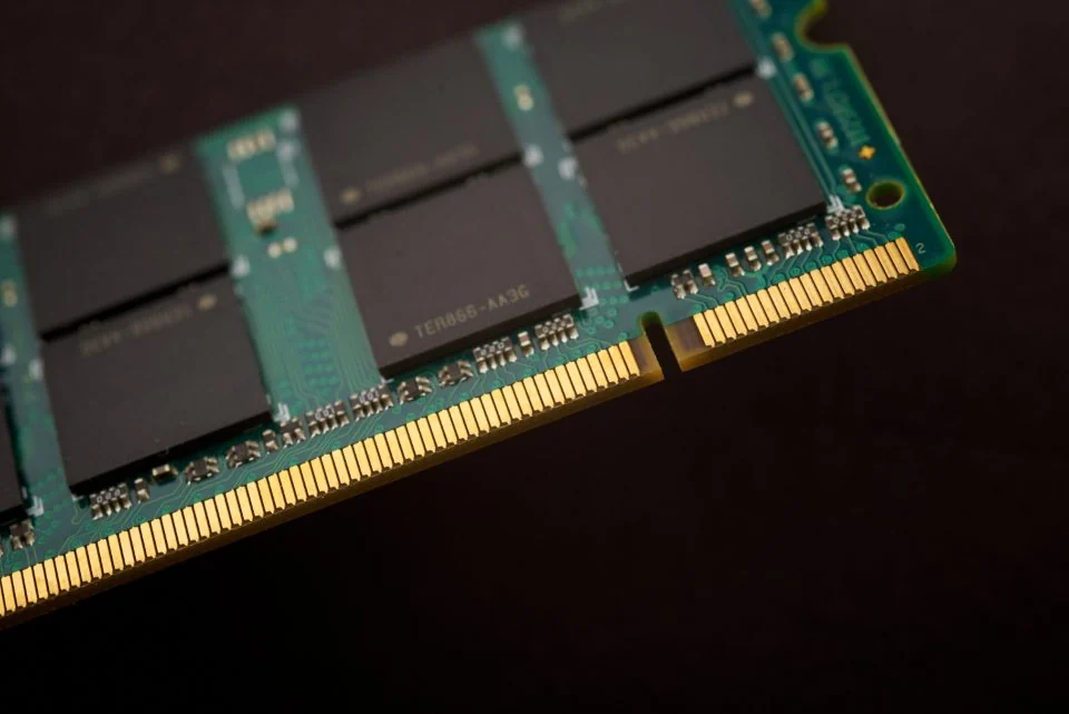
DaoAI 3D ACI equipment (proprietary 3D camera + 3D morphology reconstruction/point cloud, detecting hidden solder joints/coplanarity/micron-level morphology/voids, and other 2D optical blind spot defects, with 2D-3D fusion) precisely measures micron-level 3D morphology of semiconductor package pins, effectively replacing costly manual inspection. Production line data from a mid-sized semiconductor packaging factory indicates a reduction in labor costs for pin coplanarity and chipping inspection by over 60%, significantly improving production efficiency and product quality.
In semiconductor and chip manufacturing, pin coplanarity after packaging and chipping after dicing are critical defects affecting product reliability and subsequent assembly yield. These defects are often tiny, complex in shape, and prone to misjudgment or missed detection in traditional 2D optical inspection due to material reflectivity or shadow effects. For a long time, many semiconductor manufacturers have had to rely on time-consuming and labor-intensive manual inspection to control this quality gate, especially when facing multi-variety, small-batch production. The cost-effectiveness of manual inspection has increasingly become a significant bottleneck restricting capacity improvement and profit margins. DaoAI deeply understands this industry pain point and is committed to providing efficient automation solutions.
Pain Points: Why This Hurdle Is Difficult to Overcome
Detecting pin coplanarity and dicing chipping faces multiple challenges. Firstly, in terms of precision requirements, pin coplanarity standards are typically within tens of micrometers, and chipping defects can be as subtle as a few micrometers, far exceeding the limits of human visual acuity. Traditional rule-based AOI, due to its 2D image limitations, struggles to accurately acquire pin height information and lacks robustness for tiny chipping, leading to manual re-inspection rates of over 30% in a mid-sized packaging plant's early practices. Secondly, from a labor cost perspective, recruiting and training highly skilled inspectors is expensive, and staff turnover is high. Coupled with three-shift work models, the hourly cost of manual inspection is significantly higher than automated equipment. Production line data from this manufacturer showed that, during peak periods, manual labor costs for pin coplanarity and chipping inspection alone exceeded 200,000 RMB per month. Furthermore, manual inspection is inefficient and inconsistent, easily affected by subjective factors like fatigue and emotion, leading to fluctuating false positive and false negative rates, ultimately impacting product quality stability and production rhythm. Amidst the industrial large model trend, traditional factory quality inspection urgently needs advanced automation and intelligent solutions to address these long-standing labor cost and efficiency challenges.
The root cause of these difficulties lies in the physical characteristics of the defects and the limitations of traditional inspection methods. Pin coplanarity involves height deviations in three-dimensional space, which 2D images cannot directly measure. Dicing chipping, due to its irregular geometry and potential shadows, makes it difficult for 2D algorithms to accurately distinguish defects from normal edges. Traditional rule-based AOI often requires complex parameter adjustments and threshold settings, has poor generalization capabilities for minute defects, and consumes significant time for frequent changeovers when dealing with different batches or process parameters. All these factors make manual inspection a last resort, but its high labor costs and instability compel semiconductor manufacturers to seek more advanced automated inspection technologies. DaoAI has developed the 3D ACI equipment specifically to address these core pain points.
Technical Principles
The core of DaoAI's 3D ACI equipment lies in its self-developed high-precision 3D camera and advanced three-dimensional morphology reconstruction algorithms. The equipment uses structured light or laser triangulation principles, projecting known patterns or laser lines onto the surface of the object under test and capturing their deformation or reflection with high-resolution cameras to accurately calculate the 3D point cloud data of the object's surface. This point cloud data includes the X, Y, Z coordinates of each point, enabling micron-level 3D morphology reconstruction of semiconductor pins and chip edges. Unlike traditional 2D AOI, which relies solely on grayscale or color images for planar feature extraction, DaoAI 3D ACI equipment can directly acquire true height, angle, and edge contour information of pins, making the detection of defects such as coplanarity, warpage, bending, and minute chipping no longer limited by 2D optical blind spots. For example, for pin coplanarity, the system can directly measure the distance from the top of all pins to the reference plane and calculate their maximum height difference, achieving precise coplanarity evaluation with an actual accuracy of ±2 micrometers.
Compared to traditional manual inspection, DaoAI's 3D ACI equipment offers significant advantages. Firstly, there's a substantial improvement in detection accuracy and consistency, as machine vision is unaffected by fatigue, ensuring 100% full inspection consistency. In one case, its detection rate for micron-level chipping exceeded 99.7%. Secondly, there's a leap in detection speed; the equipment can complete 3D scanning and analysis of a single chip in milliseconds, far surpassing the cycle time of manual inspection. Furthermore, the DaoAI ACI OS operating system integrates visual foundation models and APDT positive/few-shot learning technology, allowing the equipment to complete 0-code automatic programming within 5 minutes with only 1-20 good samples when facing new products or process changes. This significantly shortens changeover times and reduces reliance on professional vision engineers. This 2D-3D fusion detection capability not only solves blind spot defects difficult for traditional 2D optics but also effectively filters out interference from ambient light and material reflections through intelligent algorithms, greatly reducing the false positive rate, making DaoAI 3D ACI an ideal choice for semiconductor quality inspection.
Typical Application Scenarios
- **Pin Coplanarity Detection:** Performs 3D scanning of pins for QFP, QFN, BGA, and other package types, accurately measuring the height difference from the top of all pins to the reference plane to determine if coplanarity standards are met. The challenge lies in the large number of pins, small spacing, and potential for minute warpage or bending. DaoAI equipment easily captures these subtle deformations through high-density point cloud reconstruction.
- **Dicing Chipping Detection:** After wafer dicing, performs 3D morphology analysis of chip edges to accurately identify and measure the size and depth of defects such as chipping and cracks. The challenge is that chipping shapes are irregular and often accompanied by material debris, which is difficult for traditional 2D to accurately distinguish. DaoAI 3D ACI equipment can precisely quantify defects from a 3D perspective.
- **Package Warpage Detection:** Measures the flatness of the entire chip package to assess stress deformation that may occur during soldering or assembly. The challenge is the need for high-precision 3D scanning of a large area. DaoAI's solution provides global high-precision morphological data.
- **Solder Joint 3D Morphology Detection:** For hidden solder joints of BGA, CSP, and other packages, analyzes key parameters such as solder joint volume, height, and wetting angle through 3D scanning to determine soldering quality. The challenge is that solder joints are located under the package body, making direct observation difficult with traditional optics. DaoAI 3D ACI combined with technologies like X-ray can achieve more comprehensive detection.
- **Micron-level Scratch and Indentation Detection:** Measures the 3D depth and width of minute scratches and indentations on the chip surface or package body. The challenge is that these defects can be very shallow and irregular. DaoAI equipment can capture their 3D features with micron-level resolution.
Case Study
A mid-sized semiconductor packaging factory, primarily producing integrated circuit products for consumer electronics and automotive electronics, relied on manual inspection and limited rule-based AOI equipment for pin coplanarity and dicing chipping detection before adopting DaoAI 3D ACI equipment. Due to rapid product iteration and numerous batches, manual inspection faced immense pressure, leading to high labor costs. During night shifts and holidays, insufficient staffing made it difficult to guarantee inspection efficiency and quality. Production line data indicated that manual inspection had a false positive rate as high as 5% and a false negative rate that could not be consistently controlled below 0.5%, severely impacting the yield of subsequent processes. To resolve this predicament, the factory decided to introduce DaoAI 3D ACI equipment, aiming for a complete replacement of manual inspection and an increase in automation levels.
The DaoAI team collaborated closely with the manufacturer, deploying multiple 3D ACI devices. In the initial phase, leveraging the APDT few-shot learning function of DaoAI ACI OS, only 15 good samples were used to quickly complete the training of detection models for various package types regarding pin coplanarity and chipping defects. The entire debugging and changeover process was completed within 30 minutes, significantly faster than the several hours or even days required for traditional AOI parameter tuning. After deployment, the DaoAI 3D ACI system quickly took over most of the previously manual inspection tasks. Production line data showed that the system effectively reduced the false negative rate for pin coplanarity and dicing chipping to <0.2%, and the false positive rate significantly dropped to <1%, reducing the workload of manual re-inspection by over 80%. More importantly, through automated inspection, the manufacturer reduced labor costs on the same production line by 65% and achieved 24/7 continuous stable operation, significantly increasing capacity and product quality stability.
“DaoAI 3D ACI equipment not only solved our long-standing high labor cost issue with manual inspection but also elevated our product quality control to an unprecedented level. This is not just an increase in efficiency but a leap in our core competitiveness.”
DaoAI Solutions and Products
DaoAI provides a core solution centered on its 3D ACI equipment, combined with the DaoAI ACI OS operating system, offering precise, efficient, and cost-effective automated quality inspection for the semiconductor industry. The 3D ACI equipment, through its self-developed high-precision 3D camera and three-dimensional morphology reconstruction technology, achieves precise capture of micron-level defects, effectively compensating for the blind spots of 2D optical inspection. Its 2D-3D fusion capability means the equipment can simultaneously utilize texture information from planar images and morphological information from 3D point clouds for more comprehensive and robust defect judgment. In terms of deployment and integration, DaoAI 3D ACI supports multiple forms such as SDK/API/Docker and can achieve 100% local private deployment, ensuring customer data security without leaving the factory, meeting the stringent requirements of the semiconductor industry for data security and compliance. Furthermore, the DaoAI ACI OS's “one good sample, 5 minutes, 0-code automatic programming” capability greatly simplifies model training and production line changeover processes, allowing non-specialized personnel to quickly get started and lowering the technical threshold for automation. DaoAI can also provide the DaoAI World global model as a unified foundation, supporting semantic understanding, cross-scenario generalization, and continuous learning and optimization from production line feedback, constantly improving the adaptability and accuracy of detection models.
The introduction of DaoAI 3D ACI equipment has enabled customers to achieve significant business value. In the aforementioned semiconductor packaging factory case, production line data shows that labor costs for pin coplanarity and dicing chipping detection were reduced by 65%. Concurrently, due to improved detection accuracy and consistency, the overall product yield increased by 2.5%, and the rework rate decreased by 15%. Moreover, automated inspection completely resolved issues related to manual inspection limitations during night shifts and holidays, enabling 24/7 continuous production, which boosted the factory's capacity by over 20%. The rapid changeover capability of DaoAI 3D ACI equipment also allowed the customer to respond more flexibly to multi-variety, small-batch production demands, enhancing market competitiveness. These quantified results fully demonstrate the immense potential of DaoAI 3D ACI solutions in replacing manual inspection and reducing labor costs.
FAQ
How does DaoAI's 3D ACI equipment achieve precise detection of micron-level defects?
DaoAI's 3D ACI equipment utilizes a proprietary high-precision 3D camera combined with structured light or laser triangulation principles to reconstruct 3D point cloud data of the object's surface. This allows for direct acquisition of micron-level 3D morphological information such as pin height, angle, and edge contours, enabling precise identification and measurement of defects often missed by traditional 2D optics, such as pin coplanarity deviations and minute chipping.
What are the cost-benefit advantages of DaoAI's 3D ACI solution compared to traditional AOI?
DaoAI's 3D ACI solution significantly reduces labor expenses by automating costly manual inspections. Furthermore, its integrated DaoAI ACI OS operating system supports 0-code rapid changeover and few-shot learning, drastically shortening production line downtime and reducing reliance on specialized vision engineers, thereby lowering overall operating and maintenance costs.
How long does it take to deploy DaoAI's 3D ACI equipment, and how is data security ensured?
Deployment time for DaoAI's 3D ACI equipment varies depending on production line complexity and integration needs, but its rapid model training capabilities (e.g., debugging completed within 30 minutes with 15 good samples) significantly accelerate the go-live process. Regarding data security, we support 100% local private deployment (SDK/API/Docker), ensuring all inspection data remains on-site and fully complies with the strict data privacy and compliance requirements of the semiconductor industry.
Full solution for this scenario: 3D ACI Equipment industry solutions
This article was generated by AI. Customer cases are simulated scenarios based on real product capabilities and figures are illustrative; see product pages for official benchmarks.