
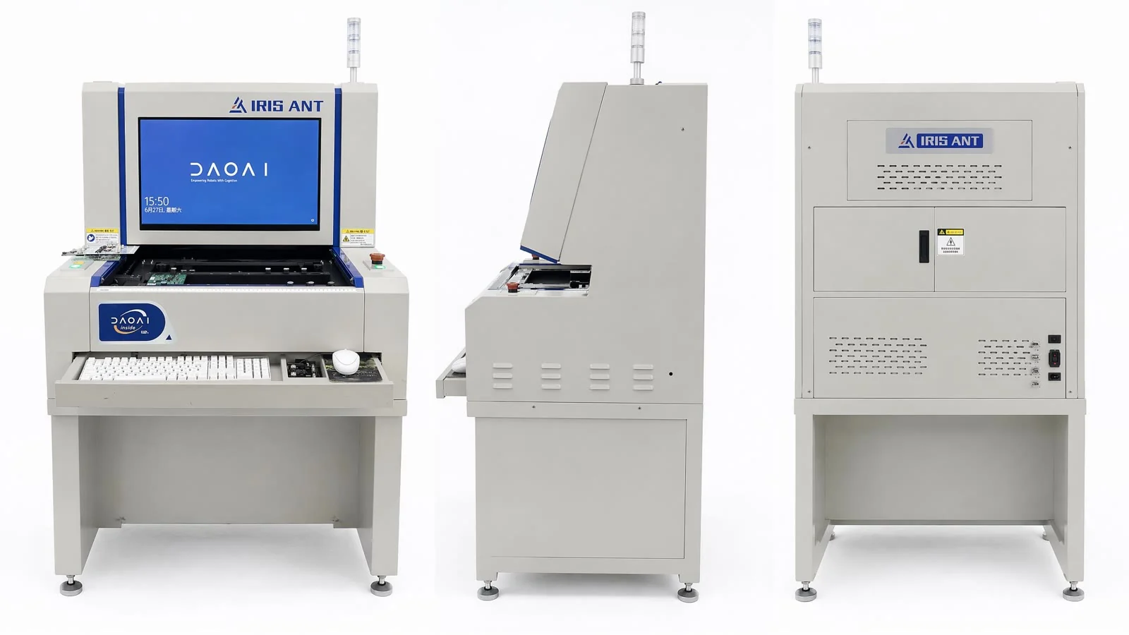
In the electronics manufacturing sector, DaoAI 3D ACI equipment (featuring proprietary 3D cameras + 3D morphology reconstruction/point cloud, capable of inspecting 2D optical blind spot defects like hidden solder joints, coplanarity, micro-scale morphology, and pores, with 2D-3D fusion) effectively addresses data security and privacy compliance challenges in hidden solder joint inspection for BGA/QFN packages through its on-premise deployment capability. It significantly reduces the false negative rate for hidden solder joints from 1.2% with traditional optical inspection to 0.08%. This breakthrough not only enhances inspection precision and efficiency but also ensures that critical production data remains within the client's premises, providing robust and reliable quality assurance for the highly sensitive electronics industry.
In the rapidly evolving field of electronics manufacturing, the quality of PCBA (Printed Circuit Board Assembly) directly determines the performance and reliability of end products. With the widespread adoption of high-density packaging technologies such as BGA (Ball Grid Array) and QFN (Quad Flat No-lead), traditional 2D optical inspection equipment faces significant challenges in detecting hidden solder joint defects within these packages. These solder joints, due to their structural characteristics, cannot be directly observed by 2D vision systems, posing potential product quality risks. A mid-sized PCBA manufacturer, whose production lines focus on high-reliability industrial control boards and communication modules, has extremely stringent requirements for solder joint quality, especially for the spherical solder joints under BGA packages between the chip and the PCB. Defects such as cold solder joints, short circuits, insufficient solder, or pores can directly lead to product failure. Simultaneously, due to involvement of core technologies and sensitive data, this manufacturer has extremely strict requirements for data security and privacy protection during the production process, rejecting any cloud-based deployment or data outsourcing solutions. This became the primary consideration when seeking advanced inspection solutions.
Pain Points: Why This Hurdle Is Difficult to Overcome
Hidden solder joint inspection in BGA/QFN packages is a major challenge in PCBA manufacturing, where traditional solutions face multiple difficulties. Firstly, **high false negative rates** persist: Traditional 2D AOI equipment cannot penetrate the chip body and has complete 'blind spots' for internal defects of BGA solder balls such as coplanarity, collapse, bridging, or voids, leading to a BGA hidden solder joint false negative rate of up to 1.2% for a certain PCBA manufacturer (production line data). Secondly, **high false alarm rates and manual re-inspection costs**: To compensate for the shortcomings of 2D inspection, production lines often have to increase detection sensitivity, resulting in a large number of false alarms. This leads to a surge in manual re-inspection hours, requiring an average of 2-3 personnel per shift for re-inspection, severely slowing down the takt time and increasing operating costs. Thirdly, **data security and compliance risks**: For clients involved in critical technologies and national security, localized storage and processing of production data (such as product designs, process parameters, and defect images) are non-negotiable. Traditional inspection solutions, if reliant on cloud services or external data processing, would introduce serious data leakage risks and compliance issues.
The root cause of these difficulties is that BGA/QFN solder joints are located beneath the package body, with the optical path completely blocked by the chip itself, preventing traditional 2D imaging technology from acquiring their 3D morphological information. Even certain specialized 2D angled cameras can only observe peripheral areas, remaining ineffective for core regions. Furthermore, the reflective properties of solder materials, their microscopic size (typically at the micron level), and the complex diversity of defects (such as micro-pores, incomplete solder wetting) all impose extremely high demands on imaging and algorithms. Considering the current hot topic of industrial large models in improving industrial vision defect recognition rates, we observe that even with powerful models, the ability to identify defects in 2D optical blind spots will ultimately be limited without high-quality, comprehensive 3D data support. DaoAI's 3D ACI equipment precisely addresses this core pain point by offering an effective solution through innovative technology.
Technical Principles
The core advantage of DaoAI's 3D ACI equipment lies in its self-developed 3D camera and advanced 3D morphology reconstruction technology. This equipment utilizes a combination of multi-frequency structured light projection and a high-resolution camera array to project a series of encoded gratings onto the BGA/QFN package area under test, simultaneously capturing reflected images. By processing these images with complex 3D point cloud algorithms, the DaoAI system can precisely reconstruct the complete 3D morphological data of hidden solder joints beneath the chip, including micron-level features such as height, volume, and coplanarity. This enables clear presentation and quantitative analysis of defects unreachable by traditional 2D optical inspection, such as BGA solder ball collapse, short circuits, voids, pores, as well as QFN package pad wetting and lead climb height. DaoAI 3D ACI combines 2D-3D fusion technology, retaining texture and color information from 2D images while acquiring high-precision 3D information, achieving comprehensive defect detection.
Compared to traditional rule-based AOI and manual inspection, DaoAI 3D ACI equipment offers significant advantages. Traditional rule-based AOI relies on preset geometric rules and brightness thresholds, making it difficult to adapt to the complex 3D morphological variations of BGA solder joints, and it cannot detect hidden defects, leading to high false negative rates. While manual inspection can identify some complex defects based on experience, it is inefficient, inconsistent, susceptible to subjective factors, and cannot perform non-destructive inspection of hidden solder joints, let alone meet the takt time requirements of high-speed production lines. In contrast, DaoAI 3D ACI acquires real 3D data, combined with the vision foundation model embedded in the DaoAI ACI OS operating system, enabling deeper feature recognition and defect analysis, significantly improving detection accuracy and stability. With on-premise deployment, all data processing and model inference are completed within the client's factory, ensuring data security and avoiding potential privacy leakage risks associated with traditional solutions.
Typical Application Scenarios
- **BGA Solder Ball Coplanarity and Collapse Detection**: DaoAI 3D ACI equipment can accurately measure the overall coplanarity of BGA solder ball arrays and identify individual solder ball collapse or excessive protrusion, which usually lead to cold solder joints or poor contact. The challenge lies in the large number of solder balls, their minute size, and their location beneath the package body, requiring extremely high 3D measurement precision.
- **BGA Solder Joint Bridging and Short Circuit Detection**: Through 3D morphology reconstruction, the DaoAI system can identify whether there is solder bridging between adjacent BGA solder balls, a critical defect causing short circuits. Traditional 2D cannot penetrate, while 3D ACI can clearly distinguish the presence of connections between solder joints.
- **QFN Package Pad Wetting and Lead Climb Height Detection**: QFN package leads are located on the sides or bottom of the package, and lead climb height and pad wetting are critical quality indicators. DaoAI 3D ACI can precisely measure the climb height and solder coverage rate of each lead, ensuring soldering strength and conductivity, and preventing open circuits or cold solder joints.
- **Hidden Solder Joint Void and Pore Detection**: Voids or pores within solder joints reduce joint strength and affect electrical conductivity and heat dissipation. DaoAI 3D ACI, through high-precision 3D point cloud data, can analyze the internal morphology of solder joints, identifying and quantifying micron-level void or pore defects, which is impossible with traditional optical inspection.
- **Insufficient or Excessive Solder Detection**: Precisely measure the volume and height of BGA/QFN solder joints to ensure that the solder volume meets process specifications, preventing cold solder joints due to insufficient solder or bridging due to excessive solder.
Implementation Case Study
A mid-sized PCBA manufacturer, primarily producing industrial-grade communication modules and controllers, has extremely high product reliability requirements. Previously, in the hidden solder joint inspection process for BGA/QFN packages, the factory mainly relied on traditional 2D AOI combined with X-Ray sampling. However, X-Ray is costly, slow, and cannot achieve full inspection, leading to a long-term BGA hidden solder joint false negative rate of around 1.2%. More importantly, this manufacturer had strict requirements for the security and local deployment of production data, ruling out all traditional cloud-based intelligent inspection solutions. After extensive evaluation, the manufacturer ultimately chose DaoAI's 3D ACI equipment for on-premise private deployment. During the deployment process, the DaoAI technical team collaborated closely with the client, integrating the 3D ACI equipment into the existing SMT production line.
After the deployment of DaoAI 3D ACI equipment, the PCBA manufacturer's BGA/QFN hidden solder joint false negative rate plummeted from 1.2% to 0.08%, while all inspection data was stored and processed locally, completely eliminating data security concerns.
Post-deployment data showed that the DaoAI 3D ACI system reduced the false negative rate for BGA/QFN hidden solder joints (including coplanarity, bridging, and pores) from 1.2% with traditional AOI to 0.08%, increasing the detection rate to 99.92%. Concurrently, due to the precision of 3D data, the false alarm rate was significantly reduced, decreasing manual re-inspection volume by 75% and greatly improving production line efficiency. More critically, all inspection data, images, and model training and inference were completed on the client's internal servers, ensuring that data never left the factory. This fully met the manufacturer's stringent requirements for on-premise private deployment.
DaoAI Solutions and Products
The core solution provided by Microchain DaoAI to this PCBA manufacturer is its 3D ACI equipment based on proprietary 3D camera technology. This equipment integrates the DaoAI ACI OS operating system, with a built-in vision foundation model that supports APDT few-shot learning. It requires only 1-20 good samples to complete 0-code automatic programming and rapid defect model establishment within 5 minutes, significantly shortening new product changeover times. For BGA/QFN packages, DaoAI 3D ACI can precisely extract key morphological features of solder joints such as height, volume, coplanarity, and porosity from 3D point cloud data, and combine them with 2D images for fused analysis, achieving comprehensive coverage of hidden solder joint defects. In terms of deployment, the DaoAI 3D ACI solution supports 100% on-premise private deployment. All computing resources, data storage, and model operations are completed within the client's factory premises, ensuring that data never leaves the facility, meeting the client's most stringent data security and compliance requirements.
Furthermore, the DaoAI 3D ACI equipment, in its on-premise deployment environment, can still leverage its powerful AI inference capabilities to perform real-time analysis of massive 3D data. Its semantic false alarm filtering function effectively reduces false alarms common in traditional rule-based detection, enhancing the overall stability and reliability of the inspection system. Through data interface integration with the client's existing MES system, DaoAI 3D ACI achieves real-time uploading and traceability of inspection data, establishing a complete quality closed-loop. The system reduced the false negative rate for hidden solder joints by 93% (from 1.2% to 0.08%), decreased manual re-inspection hours by 75%, and lowered per-unit inspection costs by 20%, while ensuring absolute security of the client's sensitive production data, bringing significant business value and competitive advantage to the client.
FAQ
How does DaoAI 3D ACI equipment ensure data security for BGA/QFN hidden solder joint inspection?
DaoAI 3D ACI equipment supports 100% on-premise private deployment. All inspection data, image acquisition, and model training and inference are completed on the customer's internal servers within the factory, ensuring that data never leaves the premises. This completely eliminates data leakage risks and guarantees data privacy and compliance.
What defects in BGA/QFN hidden solder joint inspection can DaoAI 3D ACI equipment identify that traditional 2D AOI cannot?
Leveraging its 3D morphology reconstruction capability, DaoAI 3D ACI equipment can precisely detect BGA solder ball coplanarity, collapse, bridging, voids, and pores, as well as QFN package pad wetting and lead climb height. These are defects that traditional 2D AOI cannot effectively identify due to optical blind spots.
How is the cost of deploying DaoAI 3D ACI equipment for BGA/QFN hidden solder joint inspection evaluated?
The deployment cost of DaoAI 3D ACI equipment depends on specific production line scale, inspection takt time requirements, integration complexity, and desired functional modules. We provide customized solutions and quotations based on the client's actual needs. Please contact our sales team for detailed consultation and solution evaluation to receive an accurate quote.
Full solution for this scenario: the full inspection solution for 3D ACI Equipment · Produce Ripeness Robotic Sorting: On-Premise Deployment
This article was generated by AI. Customer cases are simulated scenarios based on real product capabilities and figures are illustrative; see product pages for official benchmarks.