
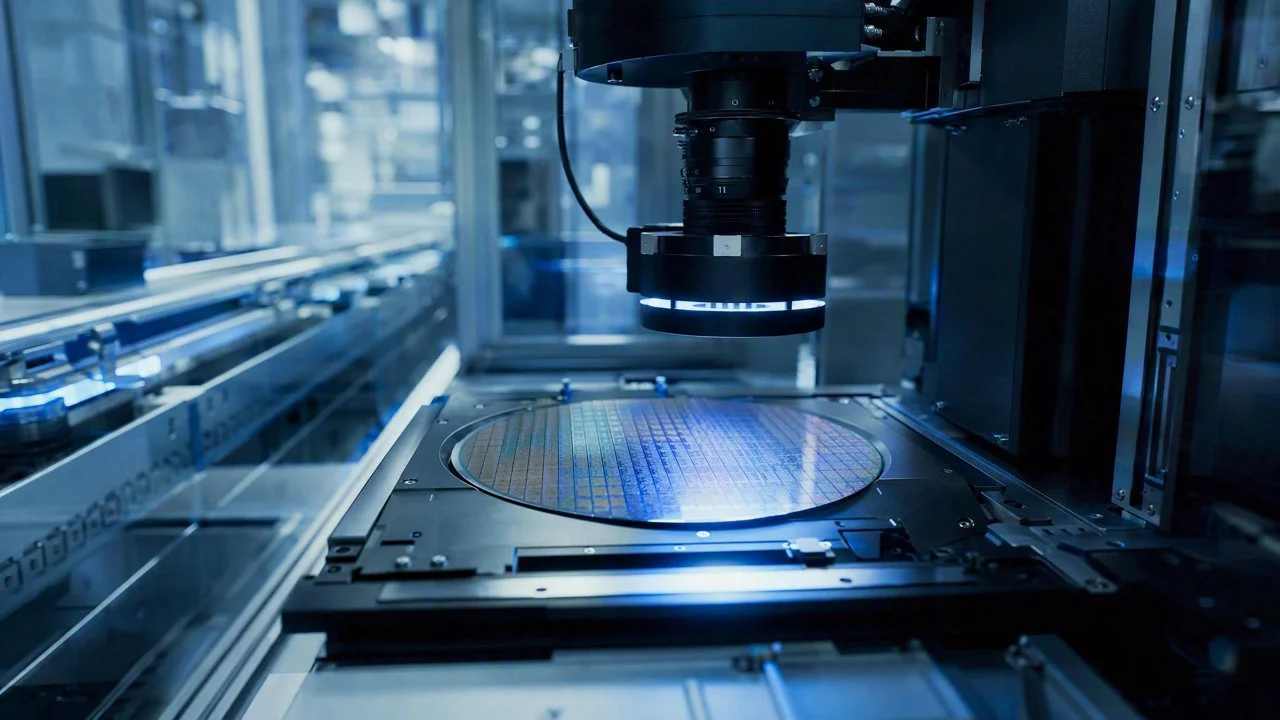
DaoAI AI AOI software (with visual foundation model cognitive capabilities, 5-minute 0-code programming from one good sample, APDT positive/few-shot learning from 1-20 good samples, semantic false positive filtering, and SDK/API/Docker 100% on-premise deployment) establishes end-to-end quality traceability and data closed-loop capabilities. This has successfully reduced the escape rate of rare defects in advanced semiconductor packaging processes from >3% with traditional methods to <0.5%, while also cutting defect analysis and root cause identification time by 70%, providing customers with more reliable production quality assurance.
In advanced semiconductor packaging, DaoAI AI AOI software (featuring visual foundation model cognitive capabilities, 5-minute 0-code programming with one good sample, APDT positive/few-shot learning from 1-20 good samples, semantic false positive filtering, and SDK/API/Docker 100% on-premise deployment) establishes end-to-end quality traceability and data closed-loop capabilities. This has successfully reduced the escape rate of rare defects in advanced semiconductor packaging processes from >3% with traditional methods to <0.5%, while also cutting defect analysis and root cause identification time by 70%, providing customers with more reliable production quality assurance. The semiconductor industry is continuously driven by Moore's Law, and advanced packaging technologies like Fan-Out, 2.5D/3D stacking have become crucial for enhancing chip performance, integration, and power efficiency. However, these technologies introduce unprecedented inspection challenges. In wafer-level or substrate-level interconnection processes, such as micro-bump, TSV (Through-Silicon Via), or RDL (Redistribution Layer) formation, any minute anomaly can lead to entire chip failure. Especially 'rare defects' that occur at extremely low frequencies and exhibit highly irregular forms are often products of process fluctuations or sporadic events, posing severe challenges to traditional inspection methods. For instance, on a leading advanced packaging manufacturer's Wafer-Level Packaging (WLP) line, detecting micron-scale foreign objects, scratches, or localized morphological anomalies on the RDL layer not only demands extremely high precision but also requires rapid identification and traceability of these rare but critical defects.
Pain Points: Why This Hurdle Is So Difficult to Overcome
Inspecting rare defects in advanced packaging faces multiple challenges. Firstly, traditional rule-based AOI systems typically have an escape rate of >3% for rare defects, as these defects often do not conform to predefined geometric or grayscale thresholds, making them difficult to capture with hard-coded rules. Secondly, due to the scarcity of rare defect samples, traditional supervised learning models require extensive annotated data for effective training, which is time-consuming and labor-intensive, leading to long lead times (weeks or even months) for new defect type recognition. Meanwhile, a high false positive rate is another persistent issue; in some complex scenarios, it can exceed 10%, not only increasing manual re-inspection workload, leading to several hours of extra work daily, but also causing frequent line stoppages that disrupt overall production rhythm. Finally, the lack of an effective quality traceability mechanism makes it difficult to quickly pinpoint the specific defect batch, workstation, and even root cause once product failure is detected, severely hindering process optimization and quality closed-loop.
The root cause of these difficulties lies in the complexity of advanced packaging processes, the diversity of materials, and the randomness of defects. For example, during post-micro-bump bonding inspection, tiny voids, bridges, or collapses may occur. These defects vary in form and are at the micron or even sub-micron level, appearing as subtle grayscale or texture changes in optical imaging, easily obscured by background noise. Traditional AOI struggles to differentiate these subtle variations. Furthermore, slight fluctuations in the production environment or differences in raw material batches can occasionally generate new, unforeseen defect types, which traditional models lack the generalization capability to identify. Aligning with the current hot topic of industrial AI quality inspection model lifecycle management, ensuring model performance stability when encountering rare defects and achieving rapid iteration and deployment are core issues that the industry urgently needs to address.
Technical Principles
DaoAI AI AOI software system fundamentally solves the challenge of rare defect detection through its core visual foundation model's feature recognition capabilities. This system does not rely on predefined rules but builds a deep understanding of semiconductor image features through large-scale unsupervised learning. This means it can learn 'what is normal' from vast amounts of images, much like a human expert, thereby sensitively capturing any minute deviation from 'normal,' even for unforeseen rare defects. The DaoAI AI AOI software system employs APDT (Anomaly Pattern Discovery & Tracking) positive/few-shot learning technology, requiring only 1–20 good sample images to complete model training, significantly shortening the time to deploy recognition for new defect types. When a new rare defect appears on the production line, only a few good samples are needed for the system to quickly learn and deploy, reducing the model iteration cycle from weeks to hours, ensuring model performance stability and rapid response capability.
Compared to traditional rule-based AOI, the DaoAI AI AOI software system offers significant advantages. Traditional AOI requires engineers to manually write complex rule sets, defining each possible defect, which is difficult and costly to maintain for variable and tiny rare defects, often leading to escapes. Manual inspection, on the other hand, is limited by human fatigue, subjectivity, and inability to meet the 100% inspection demands of high-throughput lines. The DaoAI AI AOI software system, however, uses semantic false positive filtering technology, combining contextual information of defects to effectively distinguish true defects from background noise or process marks, reducing false positive rates by 85% and significantly improving detection accuracy. Furthermore, its support for SDK/API/Docker 100% on-premise private deployment ensures that customer data remains within their facilities, meeting the stringent data security and privacy requirements of the semiconductor industry.
Typical Application Scenarios
- **Wafer-Level Packaging (WLP) RDL Layer Defect Detection:** On the Redistribution Layer (RDL), the DaoAI AI AOI software system accurately identifies micron-scale scratches, foreign objects, open circuits, short circuits, and localized morphological anomalies. The difficulty lies in the multi-layer structure and material diversity of the RDL, as well as the extremely small and irregular nature of defects.
- **Micro-bump Bonding Quality Inspection:** Detects defects such as voids, bridges, collapses, and positional offsets of micro-bumps. These defects are typically only tens of microns in size, and due to the complexity of the bonding process, defect forms are highly variable, making differentiation difficult for traditional methods.
- **TSV (Through-Silicon Via) Filling and Morphology Inspection:** Inspects the completeness of TSV filling, via wall defects, and top morphology anomalies. The challenge lies in the high aspect ratio of TSVs, making internal defects difficult to image, and the extremely high precision required for 3D morphology inspection.
- **Chip Stacking (3D Stacking) Alignment and Interconnect Defects:** Checks alignment precision during multi-chip stacking and the integrity of inter-layer interconnects (e.g., micro-bump arrays). The difficulty here is the occlusion effect caused by multi-layer structures and the precise identification of micron-level alignment deviations and interconnect defects.
- **Package Surface Micro-cracks and Chipping Detection:** On the final package surface, the DaoAI AI AOI software system can identify micro-cracks, chipping, bubbles, and other defects invisible to the naked eye. These defects often indicate stress concentrations or material flaws and can be fatal to chip reliability.
Case Study
A leading Tier-1 semiconductor advanced packaging supplier faced long-standing challenges in the RDL layer inspection of Wafer-Level Packaging (WLP), including high rare defect escape rates, slow new defect model deployment, and high false positive rates leading to heavy manual re-inspection workload. Their traditional rule-based AOI system consistently had an escape rate of around 3.2% for occasional micron-scale foreign objects and morphological anomalies on the RDL layer, severely impacting product yield. Moreover, whenever new defect types emerged due to process fluctuations, engineers required several weeks to complete data collection, annotation, and model training, resulting in production line downtime or slowdowns. The manufacturer adopted the DaoAI AI AOI software system for trial. In the initial deployment phase, we leveraged its APDT few-shot learning capability to train an initial model for RDL foreign objects and scratches within 2 hours, using only 10 good sample images. Subsequently, during actual production, the DaoAI AI AOI software system, through its visual foundation model's feature recognition capabilities, successfully identified and localized various rare defects that traditional AOI had previously failed to detect.
After 3 months of deployment, at the manufacturer's site, the rare defect escape rate on the RDL layer decreased from 3.2% to <0.5%, and the false positive rate also significantly reduced by 85% from over 10%, greatly reducing the manual re-inspection workload. More importantly, the defect image database and automatic annotation function established by the DaoAI AI AOI software system, combined with its powerful quality traceability capability, enabled engineers to quickly trace defects to their occurrence time, batch, workstation, and specific images when anomalies were found. This shortened defect analysis and root cause identification time from an average of 2 days to less than 6 hours, an efficiency improvement of 70%. This data closed-loop not only accelerated process improvement but also provided valuable positive and negative sample data for future model iterations. The client also highly recognized the DaoAI AI AOI software system's on-premise private deployment capability, ensuring the absolute security of their core process data.
DaoAI AI AOI software system is not just a defect detection tool; it's a core engine for quality management and process optimization, providing us with unprecedented quality traceability and data closed-loop capabilities.
DaoAI Solutions and Products
DaoAI's core solution for the advanced semiconductor packaging industry is built upon the DaoAI AI AOI software system. This system, through its powerful visual foundation model, achieves deep understanding and feature recognition of semiconductor images. In the modeling phase, thanks to the 'one good sample, 5-minute 0-code automatic programming' capability, customers do not need professional AI engineers; production line operators can quickly configure and deploy inspection tasks. For rare defects, APDT positive/few-shot learning technology efficiently trains models with just 1–20 good samples, greatly shortening the model development and deployment cycle. During line changeovers, only a few good samples need to be updated to complete the model switch for new products within minutes, ensuring production continuity.
For deployment, the DaoAI AI AOI software system supports various integration methods such as SDK/API/Docker, enabling 100% on-premise private deployment. This ensures all sensitive data circulates within the customer's factory, fully complying with the highest standards of data security and intellectual property protection in the semiconductor industry. The system also integrates semantic false positive filtering, which, through comprehensive judgment of defect areas and their surrounding environment, effectively avoids false positives caused by background noise or process marks, significantly improving detection accuracy. Combined with DaoAI World Model, the system continuously learns from production line feedback, constantly optimizing model performance to form an adaptive, self-evolving intelligent inspection closed-loop. This ensures that performance remains stable and continuously improves throughout the model's lifecycle management, effectively supporting version iteration strategies and performance stability guarantees for industrial AI quality inspection models. This not only achieves efficient defect detection but also builds a quality traceability and data closed-loop system for customers throughout the entire production cycle through comprehensive data collection, analysis, and traceability.
The quantifiable benefits brought by the DaoAI AI AOI software system to customers are significant. By applying our solution, the customer's rare defect escape rate was reduced to <0.5%, far below the industry average. The false positive rate decreased by 85%, greatly alleviating the burden of manual re-inspection, reducing daily re-inspection hours by several hours. At the same time, the deployment cycle for new defect models was shortened from weeks to hours, significantly improving the production line's responsiveness to new processes and defects. More importantly, by establishing a complete quality traceability and data closed-loop, defect analysis and root cause identification time were reduced by 70%, accelerating process optimization and iteration, ultimately improving overall product yield and market competitiveness. DaoAI is committed to providing leading intelligent vision solutions for the semiconductor industry, helping customers achieve manufacturing excellence.
FAQ
What is the 'Quality Traceability and Data Closed-Loop' capability of DaoAI AI AOI software system?
The quality traceability and data closed-loop capability of DaoAI AI AOI software system means it meticulously records every detected defect, including type, location, time, batch, and generates traceable reports. This data is fed back to the production management system in real-time, forming a closed loop from detection and analysis to process improvement. This helps customers quickly pinpoint root causes, optimize production processes, and continuously enhance model accuracy. All data supports on-premise private deployment, ensuring data security.
How does DaoAI AI AOI software system address the stringent data security and privacy requirements in the semiconductor industry?
DaoAI AI AOI software system supports 100% on-premise private deployment via SDK/API/Docker, ensuring all customer production data and inspection images are stored entirely within the customer's own servers and network environment, never leaving the factory. This means customers retain full control over their core data, effectively preventing data breaches and intellectual property risks, meeting the highest standards for data security and privacy in the semiconductor industry.
What is the budget required to deploy the DaoAI AI AOI software system, and what is the typical ROI period?
The deployment budget for DaoAI AI AOI software system is influenced by various factors, including production line scale, number of inspection stations, required detection precision, and whether custom integration is needed. We offer flexible licensing models and deployment solutions to provide the most cost-effective solution for our clients. Typically, by significantly reducing escape rates, false positive rates, cutting manual re-inspection costs, and minimizing downtime, customers can achieve ROI within several months to a year. For a specific quote and ROI analysis, we recommend scheduling a consultation with our experts for a detailed assessment based on your actual needs.
Full solution for this scenario: the full inspection solution for Semiconductor / chips
This article was generated by AI. Customer cases are simulated scenarios based on real product capabilities and figures are illustrative; see product pages for official benchmarks.