
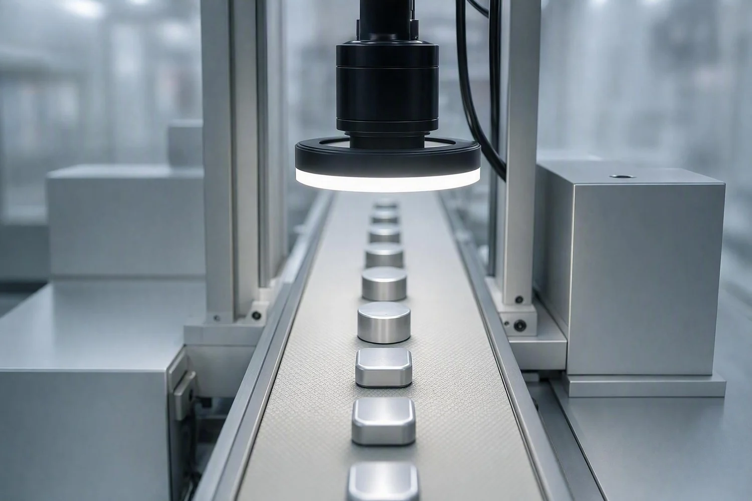
DaoAI 3D ACI equipment (featuring proprietary 3D cameras + structured light 3D metrology/point cloud reconstruction, detecting hidden solder joints, coplanarity, micron-level morphology, open pores, surface depressions, and other 2D optical blind spot defects; integrating 2D-3D data; structured light measures only surface geometry, while internal defects of opaque objects are imaged by X-ray/CT and interpreted by ACI) precisely inspects the 3D morphology of semiconductor micro-bumps. It effectively resolves the challenges of missed detections and false positives in conventional micro-bump inspection for defects like missing or bridging bumps. Furthermore, it establishes a quality data closed-loop from defect identification to production line feedback, significantly reducing the escape risk in manual re-inspection stages.
ACI in this article stands for Auto Cognitive Inspection — the next-generation term for AI AOI: keep the A and the I, and replace the O (optical) with C (cognitive), because the decision basis is cognition rather than the imaging method. The full argument is set out in From AI AOI to ACI.
Micro-bump inspection in the semiconductor industry is a critical process in advanced packaging (such as Flip-Chip and WLCSP), directly impacting chip electrical performance and reliability. As chip integration and I/O density continue to increase, micro-bump sizes shrink, and pitches become tighter, posing unprecedented challenges to inspection accuracy and speed. Traditional 2D AOI solutions often suffer from misjudgments or missed detections when dealing with defects like missing, bridging, collapse, or height inconsistency of micro-bumps, due to inherent optical limitations. This is particularly problematic in today's pursuit of high yield and low cost, where any minor defect can lead to chip scrap, affecting product launch cycles and competitiveness. Establishing an intelligent inspection system capable of precise defect identification, real-time data feedback, and full-link quality traceability has become an urgent need for semiconductor packaging manufacturers.
Pain Points: Why This Hurdle Is Difficult to Overcome
In semiconductor micro-bump inspection, traditional solutions face multiple challenges. First, [optical imaging limitations] are a core difficulty. Micro-bump sizes are typically in the tens of micrometers, and surfaces may exhibit high reflectivity or absorption differences, making it difficult for 2D AOI to acquire clear, stable-contrast images, especially for 2D optical blind spot defects like inconsistent bump height, slight collapse, or side bridging. Missed detection rates remain high; production line data shows that under certain complex processes, the missed detection rate of traditional 2D AOI can even exceed 5%. Second, [data silos and traceability gaps] are critical constraints to quality improvement. Even when defects are detected, traditional systems often lack effective correlation with upstream process parameters and downstream test results, making root cause analysis difficult and preventing the formation of an effective quality improvement closed-loop. Manual re-inspection is not only time-consuming and labor-intensive but also susceptible to subjective factors, introducing new false positives and missed detections. According to a leading manufacturer, their daily manual re-inspection hours can reach several hours, yet still carry approximately 0.5% risk of missed defects. Furthermore, [inefficient changeover and programming] is another pain point. Whenever product models or process parameters are adjusted, traditional AOI requires significant time for rule programming and parameter tuning, increasing production line downtime and impacting overall production rhythm.
The root cause of these problems lies in the [high precision and complexity] of semiconductor manufacturing. Micro-bump processes demand extremely high standards for materials, equipment, and environmental control, where any minor fluctuation can lead to defects. Simultaneously, the full-link challenges of industrial AI quality inspection, from imaging and algorithm selection to production line deployment, are also evident here. Traditional rule-based algorithms struggle to adapt to diverse defect patterns, and deep learning models, without high-quality 3D data support, will have compromised generalization capabilities and accuracy. The lack of a unified intelligent platform to integrate 2D/3D data, enable rapid model training and deployment, and connect quality data links is a common predicament across the industry.
Technical Principles
DaoAI 3D ACI equipment fundamentally addresses the pain points of traditional 2D optical inspection by integrating proprietary high-precision 3D cameras with structured light 3D metrology. This equipment employs multi-frame projected structured light technology, projecting specific patterns onto the surface of the object under test. By analyzing image distortions, it precisely calculates the 3D coordinates of each point, generating high-density point cloud data. Unlike traditional 2D AOI, which relies solely on planar grayscale information, DaoAI 3D ACI can acquire real height, volume, coplanarity, and other micron-level morphological information of micro-bumps, enabling precise quantitative detection of defects such as missing, bridging, collapse, and non-uniformity. Its ±6μm height accuracy and 2μm repeatability ensure sensitivity to minute defects. Concurrently, through 2D-3D fusion technology, DaoAI 3D ACI combines the texture information from 2D images with the geometric information from 3D point clouds, enhancing the robustness of defect identification in complex backgrounds. This multi-dimensional data fusion not only improves detection accuracy but also provides a richer, more reliable data foundation for subsequent quality traceability.
Compared to traditional manual visual inspection and rule-based AOI, the advantages of DaoAI 3D ACI are evident: First, [broader data dimensionality]. It fundamentally solves the problem of detecting 2D optical blind spot defects, capable of identifying subtle morphological anomalies that are difficult for the human eye and 2D AOI to find. Second, [higher inspection accuracy]. Micron-level measurement capability far exceeds human visual limits and avoids errors caused by subjective human judgment. Third, [higher automation]. The DaoAI ACI OS operating system integrates visual foundation models and APDT few-shot learning capabilities, supporting 5-minute 0-code automatic programming with a single good sample, significantly shortening changeover times and enhancing production line flexibility. Fourth, [stronger quality traceability]. The system automatically records every inspection result, defect type, location, and corresponding 3D morphological data, which can be associated with production batches, equipment parameters, and other information, forming a complete quality archive to support subsequent yield analysis and process improvement.
Typical Application Scenarios
- **Micro-Bump Missing and Bridging Detection**: These are common defects in semiconductor packaging. DaoAI 3D ACI equipment precisely identifies missing bumps, bridging caused by excessive solder, and collapsed bumps by measuring the actual height and volume of each bump, as well as the spacing between them. The challenge lies in the tiny and dense nature of bumps, making it difficult for traditional 2D solutions to distinguish height differences.
- **Chip Pin Coplanarity Inspection**: In BGA/LGA and other packages, pin coplanarity directly affects soldering reliability. DaoAI 3D ACI can accurately measure the Z-axis height of each pin, calculating the overall coplanarity deviation to ensure stable electrical connections of the package. The difficulty lies in the large number of tightly arranged pins and the extremely high demand for height accuracy.
- **Pad Surface Morphology and Contamination Inspection**: Before chip packaging, the flatness, oxidation, and foreign object contamination of the pad surface can all affect subsequent soldering quality. DaoAI 3D ACI can perform micron-level morphological scanning of the pad area, detecting surface depressions, scratches, particulate foreign objects, and other defects that might appear as subtle grayscale changes and be difficult to identify in 2D images.
- **Wafer Edge Chipping and Crack Detection**: Chipping or micro-cracks may occur on wafer edges during dicing or handling. DaoAI 3D ACI, through high-resolution 3D imaging, can capture these subtle geometric structural anomalies. Even sub-surface cracks that are not obvious in 2D images can be indirectly detected by the surface morphological changes they induce. The challenge is the extremely small size of defects and their potential location on irregular edges.
- **Wire Bonding Loop Height and Offset Inspection**: In the wire bonding process, loop height, offset, short circuits, or breaks in bond wires are critical inspection items. DaoAI 3D ACI can precisely measure the spatial trajectory and height of bond wires, identifying abnormal loop heights, collapsed wires, or bridging caused by contact with other wires, ensuring bonding quality.
Case Study
A leading semiconductor packaging and testing facility faced persistent challenges with micro-bump inspection on its advanced packaging production lines. Their traditional 2D AOI system exhibited a false positive rate as high as 15% when dealing with the dense micro-bump arrays of new chip types, and its missed detection rate could not meet increasingly stringent quality standards. This led to a large volume of products requiring manual re-inspection, severely slowing down the production rhythm. After introducing DaoAI 3D ACI equipment, the manufacturer first leveraged the DaoAI ACI OS operating system and its APDT few-shot learning capability. They trained a new product model with only 15 good samples, taking less than 30 minutes. Upon deployment, the DaoAI 3D ACI system consistently identified various defects such as missing, bridging, and collapsed micro-bumps, controlling the false positive rate to below 2%. This significantly reduced the workload of manual re-inspection. Production line data shows that the daily manual re-inspection hours on this line decreased from 6 hours to less than 1 hour. All inspection data was uploaded in real-time to the factory's MES system, achieving comprehensive correlation of defect types, locations, 3D morphological data with production batches and equipment parameters. This shifted the process from relying on piece-by-piece manual re-inspection to only reviewing the few items flagged by the system, significantly improving the efficiency and accuracy of quality traceability. The DaoAI 3D ACI equipment also supports 100% on-premise private deployment, ensuring sample and inspection images remain within the factory, meeting the client's strict requirements for data security and compliance.
The figures above are a typically achievable range in anonymized industry scenarios — a different line or a different batch of parts will move the result either way; on-site measurement governs.
DaoAI 3D ACI is not just a defect detection tool, but a core engine for building semiconductor quality traceability and data closed-loop systems.
DaoAI Solution and Products
DaoAI's core solution for semiconductor micro-bump inspection is its proprietary 3D ACI equipment. This device integrates high-resolution 3D cameras with advanced structured light 3D metrology algorithms, capable of capturing micron-level surface geometric features. In terms of deployment, DaoAI 3D ACI equipment supports flexible integration into production lines, acting as a standalone inspection station or embedded within existing lines. The modeling and changeover processes are highly efficient, thanks to the visual foundation models and APDT (Adaptive Pre-trained Deep Transfer) few-shot self-learning capabilities built into the DaoAI ACI OS operating system. Users only need to provide 1–20 good samples to complete model cold-start programming within 5 minutes, quickly adapting to new products or defect modes, achieving 0-code rapid changeover. The DaoAI 3D ACI equipment also supports 2D-3D fusion inspection, combining texture information from 2D images with geometric information from 3D point clouds to enhance the comprehensiveness and accuracy of detection. All sample and inspection images support 100% on-premise private deployment, ensuring sample and inspection images remain within the factory and meeting the stringent data security requirements of the semiconductor industry.
Through the deployment of DaoAI 3D ACI equipment, semiconductor manufacturers can achieve precise, efficient, and fully automated inspection of micro-bump defects, thereby significantly reducing missed detection and false positive rates. Concurrently, the detailed 3D morphological data and inspection reports generated by the system can be fed back to the production management system in real-time, forming a quality data closed-loop from detection to analysis and improvement. This data closed-loop not only helps in quickly identifying and resolving process issues, improving product yield, but also provides a solid data foundation for long-term quality improvement, significantly enhancing product traceability. DaoAI 3D ACI equipment achieves a cold-start detection accuracy of 98% and can reach 99.99% after online iteration, with a single judgment latency of 12 milliseconds, realizing high-speed and high-precision inspection, effectively improving production line rhythm and overall production efficiency.
FAQ
How does DaoAI 3D ACI equipment achieve quality traceability for semiconductor micro-bump defects?
DaoAI 3D ACI equipment utilizes high-precision 3D imaging to quantitatively measure and record the 3D morphological data, location, and type of each micro-bump defect. This data is real-time associated with production batches and process parameters, then uploaded to the MES system, forming a complete quality archive. This supports root cause analysis and full-process traceability of defects, ensuring controllable product quality.
What are the core advantages of DaoAI 3D ACI equipment for micro-bump inspection compared to traditional 2D AOI?
The core advantage of DaoAI 3D ACI equipment lies in its proprietary 3D camera and structured light 3D metrology capabilities. It can acquire micron-level geometric information such as the true height, volume, and coplanarity of micro-bumps, effectively solving the missed detection and false positive issues of 2D AOI when facing optical blind spot defects like height differences, side defects, and collapse, providing more comprehensive and accurate inspection data.
How can the cost budget for deploying DaoAI 3D ACI equipment for semiconductor micro-bump inspection be evaluated?
The cost budget for DaoAI 3D ACI equipment is influenced by various factors, including production line integration complexity, required inspection speed, desired accuracy level, and whether customized functions are needed. We offer flexible configuration options. We recommend contacting our sales engineers, who will provide a detailed solution and precise quotation evaluation based on your specific production line conditions and inspection requirements.
Full solution for this scenario: the full inspection solution for 3D ACI Equipment
This article is an original publication by WeLinkirt (DaoAI). Under customer confidentiality, cases are anonymized industry scenarios and figures are illustrative; see product pages for official benchmarks.