
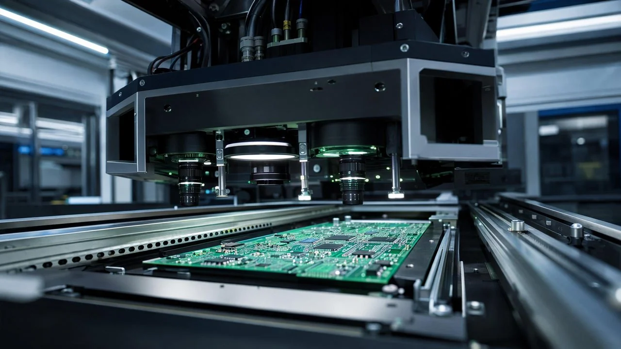
DaoAI 3D ACI equipment (proprietary 3D camera + 3D morphology reconstruction/point cloud, detecting hidden solder joints/coplanarity/micron-level morphology/voids, and other 2D optical blind spot defects, with 2D-3D fusion) significantly enhances PCBA assembly quality control by precisely reconstructing 3D morphology and integrating deep learning for defect discrimination, reducing the escape rate of micron-level voids in hidden solder joints under BGA/QFN packages from 2.5% to below 0.4%.
In the field of electronics manufacturing, the quality of PCBA (Printed Circuit Board Assembly) directly determines the reliability and lifespan of end products. As electronic products trend towards miniaturization and high integration, advanced packaging technologies such as BGA (Ball Grid Array) and QFN (Quad Flat No-leads) are widely adopted. These packages feature solder joints located beneath the package body, forming 'hidden solder joints,' which pose significant blind spots for traditional 2D optical inspection methods. Particularly for micron-level voids within BGA solder balls and subtle deviations in solder joint morphology, these defects, though imperceptible to the naked eye, can lead to cold solder joints, short circuits, or even failures during product operation, posing potential risks to product reliability. How to efficiently and accurately detect these hidden and minute defects is a critical challenge for PCBA manufacturers and a crucial step in the industrial AI deep-water zone, building enterprise-grade token pipelines for scalable application.
Pain Points: Why This Hurdle is Difficult to Overcome
Micron-level defect detection for hidden solder joints under BGA/QFN packages in PCBA faces multiple challenges, leading to high escape rates and costly manual re-inspections. Firstly, at the process level, the formation of voids within BGA solder balls is influenced by various factors such as reflow profiles, solder paste composition, and printing quality, resulting in diverse and random defect morphologies. For QFN packages, where side and bottom pads connect, subtle morphological deviations like solder joint coplanarity and fillet height are critical for product reliability but extremely difficult to detect with traditional methods. Secondly, at the imaging level, due to package obstruction, 2D AOI cannot directly observe the complete solder joint morphology beneath BGA balls or QFN bottom pads, relying instead on indirect inferences from edge contours or shadows, leading to an escape rate as high as 2.5%. Even X-Ray inspection, while capable of penetrating solder joints, suffers from complex image processing, limited precision for micron-level void identification, high inspection costs, and slow cycle times, making it unsuitable for high-volume production lines. Furthermore, traditional rule-based AOI systems have poor generalization capabilities for new defect patterns, and changeover programming is time-consuming, requiring hours or even days of manual intervention for each new product launch or process adjustment, severely impacting production efficiency.
These root causes collectively define the 'deep water zone' of inspection. Traditional methods struggle to build an effective 'enterprise-grade token pipeline' for scalable identification of these complex, hidden defects. Manual visual inspection is not only inefficient and prone to subjective errors but also inadequate for micron-level defects. The consequences of high escape rates include product rework, recalls, and even damage to brand reputation. Statistics from a leading Tier-1 consumer electronics supplier showed that product rework rates due to BGA/QFN solder joint defects once reached 1.8%, costing millions of dollars annually. Addressing these pain points fundamentally, achieving automated, high-precision, and highly generalizable defect detection, is key to upgrading modern electronics manufacturing.
Technical Principles
The core of DaoAI's 3D ACI equipment lies in its proprietary 3D camera and advanced 3D morphology reconstruction technology, combined with 2D-3D fusion deep learning algorithms. The equipment employs high-resolution structured light projection, casting multi-angle, multi-phase grating patterns onto the inspected PCBA surface. Proprietary high-speed industrial cameras simultaneously acquire images. These images undergo sub-pixel precise matching and triangulation algorithms to reconstruct a complete 3D morphological point cloud of the PCBA surface, including BGA/QFN packages and their underlying solder joints, with micron-level accuracy in milliseconds. This method overcomes the occlusion limitations of traditional 2D optics, directly obtaining precise morphological features such as 3D dimensions, height, volume, coplanarity, and internal voids of solder joints. For BGA solder ball voids, we perform voxelization and deep learning segmentation on 3D point cloud data to identify the exact location, size, and shape of micron-level cavities. For QFN pads, it can accurately measure critical but subtle morphological deviations like fillet height and lead coplanarity, which are not quantifiable from 2D images.
Unlike traditional rule-based AOI that relies on predefined thresholds and manual feature extraction, DaoAI 3D ACI equipment uses the DaoAI ACI OS, which incorporates a vision foundation model. Through APDT positive/few-shot learning mechanisms, it can achieve 0-code automatic programming in just 5 minutes with only 1-20 good samples. The system extracts a vast array of features from 3D point clouds and 2D texture images, then performs deep learning training via a 2D-3D fusion network. This enables the equipment to not only accurately identify known defects but also exhibit strong generalization capabilities for novel or variant defect patterns. For instance, for BGA solder ball voids, traditional methods can only infer indirectly via grayscale differences, susceptible to background interference; 3D AOI directly measures the 3D volume and depth of voids, combined with an AI model to determine if they constitute a defect. Furthermore, the semantic false positive filtering mechanism, by understanding contextual information in images, significantly reduces false alarms caused by process fluctuations or non-defect features, thereby cutting down manual re-inspection workload. This deep integration of 3D perception and AI-driven intelligent judgment is unparalleled by traditional methods.
Typical Application Scenarios
- **BGA Solder Ball Morphology and Void Detection**: For solder balls beneath BGA packages, the equipment reconstructs their complete external morphology, height and volume; micron-level voids inside the ball in 3D, using an AI model to precisely identify and quantify the size, location, and volume of voids. The difficulty lies in the randomness and minuteness of voids, which 2D cannot reach, and X-Ray image recognition has limited precision.
- **QFN Lead Coplanarity and Fillet Height Inspection**: QFN package pads are located at the bottom and sides of the chip; deviations in lead coplanarity and insufficient or excessive solder fillet height can affect electrical connections. 3D ACI precisely measures the height difference of each lead relative to the datum plane and the solder climb height, ensuring coplanarity and soldering quality. The difficulty lies in the small lead size, and traditional 2D cannot provide height information.
- **Hidden Solder Joint Bridging and Short Circuits**: For potential bridging between solder joints or short circuits with adjacent pads under BGA/QFN packages, the equipment analyzes 3D point clouds with high precision to identify abnormal solder connections in 3D space, even detecting minute solder balls or overflow. The difficulty lies in package obstruction, and tiny short circuits are hard to detect through electrical testing.
- **BGA Solder Ball Missing/Misalignment/Collapse**: 3D ACI accurately detects morphological anomalies such as missing, severely misaligned or excessively collapsed BGA solder balls. By comparing with a standard 3D model, these defects are quickly located and quantified. The difficulty lies in traditional 2D's reliance on indirect features, susceptible to shadow interference.
- **Micron-level Foreign Objects and Scratches**: During PCBA assembly, tiny foreign objects (e.g., metal shavings, fibers) or board surface scratches can cause short circuits or affect reliability. 3D ACI can reconstruct micron-level surface morphology, identifying and locating these subtle foreign objects or scratches, improving board cleanliness inspection. The difficulty lies in the small size and diverse morphology of foreign objects, and traditional 2D is sensitive to lighting.
Implementation Case Study
A leading Tier-1 consumer electronics manufacturer, whose smartphone motherboard PCBA production line extensively uses BGA and QFN packaged chips, faced challenges. Before integrating DaoAI's 3D ACI equipment, their production line relied on traditional 2D AOI combined with X-Ray sampling for BGA/QFN solder joint quality control. However, 2D AOI was almost incapable of detecting micron-level voids inside BGA solder balls and subtle coplanarity deviations of QFN leads, leading to persistently high escape rates and a rework rate that once reached 1.8%. While X-Ray sampling could detect some internal defects, its slow inspection cycle prevented 100% full inspection, and its precision for identifying tiny voids was insufficient, resulting in a high false alarm rate. This necessitated 3-4 quality engineers daily for extensive manual re-inspection, consuming significant man-hours and management costs. The client urgently needed a solution capable of high-precision, high-efficiency, and full-coverage inspection to meet increasingly stringent product quality requirements and rapid production iterations.
The DaoAI team deployed multiple 3D ACI devices tailored to the client's specific needs, deeply integrating them with the client's MES system. In the initial phase, we used a small amount of good sample data provided by the client (only 10-15 images per BGA/QFN package) to complete the preliminary AI model training in 5 minutes. Through continuous online learning and data feedback, the model's ability to recognize various complex defects steadily improved. In operation, the equipment achieved 100% full inspection, consistently detecting BGA solder ball internal voids larger than 50 microns in diameter and QFN lead coplanarity deviations smaller than 10 microns. After three months of trial operation and data validation, the escape rate for BGA/QFN hidden solder joint defects on this production line decreased from the original 2.5% to below 0.4%, and the false alarm rate also dropped from 6% to 1.8%. Manual re-inspection workload was reduced by 63%, significantly improving the overall OEE (Overall Equipment Effectiveness) of the production line.
"DaoAI 3D ACI not only solved our long-standing BGA/QFN solder joint inspection challenges but also, through its powerful AI learning capabilities, propelled our production line quality control into a new phase. We now have greater confidence in product reliability."
DaoAI Solution and Products
DaoAI provides a core solution based on its 3D ACI equipment for BGA/QFN hidden solder joint inspection. This system centers on a proprietary 3D camera, combining high-precision structured light projection and 3D morphology reconstruction technology to achieve micron-level 3D data acquisition of PCBA surfaces and solder joint interiors. Building on this, the DaoAI ACI OS acts as the brain, leveraging its powerful vision foundation model and 2D-3D fusion deep learning algorithms to automatically learn defect features from vast amounts of 3D point cloud and 2D texture data. The modeling process is highly automated, requiring only 1-20 good samples for model training, enabling 0-code automatic programming and significantly reducing new product introduction and changeover times to within 5 minutes. Deployment is flexible, supporting SDK/API/Docker, and allows 100% local private deployment, ensuring data security within the factory. Furthermore, through the unified DaoAI World model foundation, the system continuously learns from production line feedback, achieving cross-scene generalization and model iterative optimization.
The deployed 3D ACI equipment not only focuses on BGA/QFN hidden solder joints but can also extend to other critical inspection stages in PCBA production, such as solder paste volume and PAD coplanarity after SMT printing, as well as component placement offset, tombstoning, wrong parts, and missing parts after reflow soldering. By integrating 2D-3D inspection, it effectively compensates for the shortcomings of traditional 2D AOI in acquiring 3D information like height, volume, and coplanarity, forming a comprehensive, efficient, and intelligent PCBA quality control system. Combined with DaoAI Robot Vision, it can even achieve automatic defect picking, rework, or assembly guidance in the future. By building such an 'enterprise-grade token pipeline,' complex inspection logic and experience are transformed into reusable, scalable AI models, allowing quality control capabilities to be rapidly replicated across different production lines and product models, achieving true scalable application.
Quantified Results
By deploying DaoAI 3D ACI equipment, the client's PCBA production line achieved significant improvements in quality and efficiency, with the following quantified results:
- **BGA/QFN Hidden Solder Joint Void Escape Rate**: Reduced from 2.5% to <0.4%.
- **Inspection False Alarm Rate**: Reduced from 6% to 1.8%.
- **Manual Re-inspection Workload**: Reduced by 63%.
FAQ
How does DaoAI 3D ACI equipment detect hidden solder joint defects under BGA packages?
Our equipment utilizes a proprietary 3D camera and structured light technology to reconstruct the precise 3D morphology of BGA solder balls. Combined with 2D-3D fusion deep learning algorithms, it can directly identify and quantify micron-level voids, solder ball collapse, and misalignment within the solder balls, effectively overcoming 2D optical blind spots.
What is the detection accuracy of this equipment for QFN package solder joint coplanarity or fillet height?
For QFN packages, the 3D ACI equipment can achieve solder lead coplanarity detection accuracy of less than 10 microns and precisely measure fillet height. Through 3D point cloud data, it provides complete height and morphological information unavailable to traditional 2D AOI, ensuring soldering quality.
How many samples and how much time are needed for AI model training with DaoAI 3D ACI?
Leveraging the APDT few-shot learning capability of the DaoAI ACI OS, our equipment typically requires only 1-20 good sample images to complete 0-code automatic programming and model training within 5 minutes, significantly reducing new product introduction and changeover times.
Full solution for this scenario: Semiconductor / chips industry solutions
This article was generated by AI. Customer cases are simulated scenarios based on real product capabilities and figures are illustrative; see product pages for official benchmarks.