
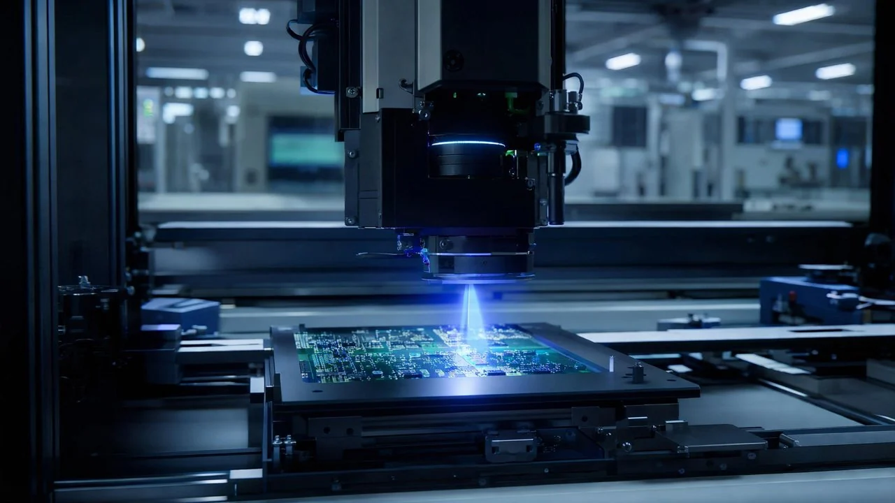
In the electronics manufacturing sector, with the proliferation of high-density packaging technologies like BGA, traditional 2D AOI equipment faces significant challenges in detecting hidden solder joints, micrometer-sized morphology defects, and internal voids beneath BGA packages. DaoAI 3D ACI equipment (proprietary 3D camera + 3D morphology reconstruction/point cloud, detecting hidden solder joints/coplanarity/micrometer morphology/voids, and other 2D optical blind spot defects, with 2D-3D fusion) effectively addressed the leakage detection of micrometer-sized voids in BGA package bottom solder joints for a leading PCBA manufacturer by combining high-precision 3D imaging with advanced AI algorithms, reducing the leakage rate for this defect from 1.2% to below 0.05%, significantly improving product quality and reliability.
DaoAI 3D ACI equipment (proprietary 3D camera + 3D morphology reconstruction/point cloud, detecting hidden solder joints/coplanarity/micrometer morphology/voids, and other 2D optical blind spot defects, with 2D-3D fusion) effectively addressed the leakage detection of micrometer-sized voids in BGA package bottom solder joints for a leading PCBA manufacturer through deep learning and 3D data analysis, reducing the leakage rate for this defect from 1.2% to below 0.05%. In the electronics/PCBA industry, with the increasing demand for high-performance, high-reliability products in consumer electronics, servers, and automotive electronics, high-density packaging technologies such as BGA (Ball Grid Array) and QFN (Quad Flat No-lead) have become prevalent. These packaging forms are characterized by dense, miniature solder joints, with BGA solder joints located at the bottom of the component, creating 'hidden solder joint' areas that are difficult for traditional 2D optical inspection methods to effectively access and evaluate. A leading PCBA manufacturer, producing high-end server motherboards, particularly focused on the welding quality of BGA packages, especially the presence of micrometer-sized voids within solder balls and whether the 3D morphology of the solder joints met standards. These defects directly impact signal integrity, heat dissipation performance, and long-term reliability, easily leading to product failure, especially in high-temperature, high-humidity environments. The client's production line utilized high-speed SMT placement processes, demanding extremely high inspection speed and precision, which traditional inspection solutions could no longer meet for their stringent quality control standards.
Pain Points: Why This Hurdle Was Difficult to Overcome
This leading PCBA manufacturer faced multiple challenges in BGA solder joint inspection: Firstly, the leakage rate of micrometer-sized voids remained stubbornly high, consistently around 1.2%, leading to increased rework and scrap rates in subsequent functional testing, adding approximately 8% to overall production costs. Secondly, the labor cost for manual re-inspection of BGA defects was extremely high, requiring an additional 3-5 person-hours per batch for X-Ray sampling and manual visual inspection, which was inefficient and could not meet the demands of high-throughput production. Thirdly, frequent changeover debugging led to an increase in production line downtime by approximately 15%, impacting overall OEE (Overall Equipment Effectiveness). The root cause of this predicament was that traditional 2D AOI could only acquire planar grayscale images, unable to penetrate the BGA component itself, making it impossible to determine the 3D morphology, volume, coplanarity, and internal voids of its bottom solder joints. Even some AOI systems with integrated 2.5D capabilities could only indirectly infer these issues through shadows or brightness changes, with accuracy and reliability far below actual needs. While X-Ray inspection could visualize internal structures, it was costly, slow, and required professional interpretation, making 100% online full inspection difficult. The current bottleneck in domestic servo drives is not merely a chip shortage; a deeper reason lies in the lagging iteration of algorithms. In areas such as precision motion control and high-accuracy positioning, the real-time, robustness, and adaptability requirements for algorithms are extremely high. This is similar to the demands for accuracy and generalization capabilities of image processing and defect recognition algorithms in the AOI field. When traditional rule-based algorithms face complex 3D structures and tiny defects in BGAs, their lack of generalization ability and difficulty in parameter tuning become apparent, leading to missed detections and false positives, unable to continuously iterate and optimize through massive data like advanced AI algorithms, thus entering a bottleneck.
Technical Principles
The core of DaoAI 3D ACI equipment lies in its proprietary high-precision 3D camera and advanced 3D morphology reconstruction algorithms, combined with 2D-3D fusion deep learning defect recognition technology. We employ multi-frequency fringe projection profilometry (FPP) or multi-angle structured light projection technology, projecting a series of encoded light stripes onto the PCBA surface with precisely controlled digital gratings. High-resolution industrial cameras then synchronously capture the deformed stripe images from different angles. These images contain the 3D morphological information of the object's surface. Subsequently, proprietary 3D morphology reconstruction algorithms perform complex phase unwrapping, triangulation, and point cloud fusion processing on the acquired images, ultimately generating high-precision, high-density 3D point cloud data. This point cloud data not only includes the X, Y, Z coordinates of each solder joint but also accurately records its height, volume, coplanarity, and surface texture at a micrometer level. For detecting internal voids in BGA solder joints, the equipment combines texture features from high-resolution 2D images with height/volume anomalies from 3D point clouds. Through deep learning models, particularly the visual foundation models within our DaoAI ACI OS, the system can learn the normal 3D morphology and texture features of solder joints from massive good product data and identify areas with significant deviations from these features. For example, micrometer-sized voids may appear as local tiny depressions or irregular surface structures in 3D morphology, and as subtle shadows or texture changes under specific lighting in 2D images. Through 2D-3D fusion, the AI model can make comprehensive judgments, avoiding misjudgments based on single-dimension information. Compared to traditional rule-based AOI, its advantage lies in not requiring manual setting of complex geometric rules and thresholds; instead, it automatically extracts defect features through learning, demonstrating stronger generalization ability and robustness to subtle variations and novel defects. Compared to manual visual inspection, it completely eliminates subjective judgment errors and fatigue caused by long working hours, achieving 100% online full inspection and high consistency.
Furthermore, our system integrates the DaoAI ACI OS, supporting APDT positive/few-shot learning, enabling rapid detection model establishment with just 1-20 good product images, significantly shortening programming time for new product introduction and changeovers. Semantic false positive filtering mechanisms effectively distinguish between process variations and true defects, further reducing false positive rates.
Typical Application Scenarios
- **Micrometer Void Detection in BGA Solder Balls**: This is the core pain point of this case. The 3D ACI equipment can accurately measure the volume and surface integrity of BGA solder balls through 3D morphology reconstruction. Micrometer voids lead to local volume anomalies or tiny depressions on the solder ball surface. These subtle morphological changes, imperceptible in 2D images, appear as clear abnormal points or regions in 3D point cloud data. After training, the AI model can precisely identify and locate these voids, ensuring defect-free solder joint interiors.
- **3D Morphology Evaluation of Hidden Solder Joints in BGA/QFN**: For solder joints at the bottom of BGA and QFN components, traditional 2D AOI cannot directly image them. Our 3D camera, through specific-angle structured light projection and reconstruction, can acquire complete 3D morphology data for these hidden solder joints, including solder volume, wetting angle, pad coverage, etc. The AI model can judge whether solder joints meet IPC standards based on these 3D parameters, for example, detecting open circuits, bridges, or tombstoning.
- **Component Lead Coplanarity Inspection**: For leads of QFN, SOP, PLCC, and other packages, their coplanarity directly affects soldering reliability. 3D ACI can precisely measure the height of all leads and calculate their coplanarity deviation, ensuring all leads are within the same plane, avoiding soldering defects caused by lead deformation or warping.
- **PCB Warpage and Reference Plane Measurement**: Before SMT placement or after reflow soldering, the warpage of the PCB itself can affect soldering quality. The 3D ACI equipment can perform 3D scanning of the entire PCB surface, generating high-precision reference plane data, used for subsequent inspection correction or as feedback to the placement machine, ensuring precise component placement and soldering.
- **Height and Tilt Detection of Irregular Components**: For irregular components such as connectors, capacitors, and inductors, their height and tilt are important assembly quality indicators. 3D ACI can accurately measure the Z-axis height and X/Y-axis tilt angles of these components, promptly identifying defects such as misalignment, floating, or tilting, ensuring product assembly quality.
Implementation Case Study
A leading PCBA manufacturer, as a Tier-1 supplier, has extreme quality control requirements for its high-end server motherboard product line. Before introducing DaoAI 3D ACI equipment, this production line faced severe challenges in BGA package inspection. They primarily relied on traditional 2D AOI for initial inspection, with very limited detection capabilities for BGA bottom solder joints and micrometer voids, resulting in a leakage rate of up to 1.2% for micrometer voids in BGA solder joints. To compensate for this deficiency, the production line had to additionally configure two X-Ray machines for sampling inspection and assign multiple senior engineers for manual re-inspection and rework. This not only incurred huge labor costs and equipment investment but also severely slowed down the overall production rhythm. More importantly, undetected defects would flow downstream, leading to product discovery and rework during the functional testing phase, and even a very small number of products entering the market experiencing early failure, severely damaging brand reputation. After in-depth discussions with the DaoAI team and multiple on-site tests, the manufacturer decided to deploy DaoAI 3D ACI equipment on one of its BGA-intensive motherboard production lines. The online process was smooth and efficient. Our engineers utilized the APDT few-shot learning function of the DaoAI ACI OS, completing the training and deployment of the defect recognition model in less than 30 minutes, using only 15 good BGA solder joint data samples. The system was smoothly integrated with the existing MES system, enabling real-time upload and traceability of inspection data. After going online, the equipment's excellent performance was immediately apparent: the leakage rate of micrometer voids in BGA solder joints plummeted from 1.2% to below 0.05%, and the detection rate increased to 99.95%. The false positive rate was also effectively controlled through semantic false positive filtering technology, reducing by approximately 63%. The production line no longer required full X-Ray sampling, and manual re-inspection was significantly reduced, saving substantial human resources and time. At the same time, new product changeover time was shortened from several hours to less than 5 minutes, greatly enhancing the flexibility and efficiency of the production line. The client highly recognized this cooperation and plans to promote deployment on more production lines.
DaoAI 3D ACI not only solved our persistent problem of missed micrometer voids in BGA solder joints but also elevated our production line efficiency and quality control to a new level. Its few-shot learning capability and rapid changeover features truly embody the value of industrial AI.
The figures above are a typically achievable range in anonymized industry scenarios — a different line or a different batch of parts will move the result either way; on-site measurement governs.
DaoAI Solution and Products
The core solution provided by DaoAI to this leading PCBA manufacturer was its 3D ACI equipment, which integrates our proprietary high-precision 3D camera and advanced 3D morphology reconstruction technology. Combined with the DaoAI ACI OS, this system is based on visual foundation models for feature recognition and possesses APDT positive/few-shot learning capabilities, enabling high-precision model training with only 1-20 good samples. For complex defects such as micrometer voids in BGA solder joints, hidden solder joint morphology, and coplanarity, the system employs a 2D-3D fusion inspection strategy, fully utilizing geometric features like height, volume, and roughness from 3D point cloud data, combined with texture and color information from 2D images, to build robust defect recognition models. In terms of deployment, our equipment supports 100% local private deployment, with data remaining on-site, fully complying with the client's strict requirements for data security and privacy. The system provides various integration methods such as SDK/API/Docker, allowing flexible embedding into the client's existing MES, SPC, and other production management systems, enabling real-time sharing and traceability of inspection data. Furthermore, DaoAI can also provide the DaoAI World Model, serving as a unified AI foundation with semantic understanding and cross-scenario generalization capabilities, capable of continuously learning from production line feedback to optimize inspection performance, providing long-term technical support for the client's future intelligent manufacturing upgrades. Through this comprehensive solution, we helped the client achieve automated, intelligent, and high-precision BGA solder joint inspection, thoroughly solving blind spot defect issues that traditional methods could not address.
Ultimately, the client not only achieved significant improvements in product quality but also realized substantial optimization in production efficiency, cost control, and risk management. DaoAI 3D ACI equipment, with its excellent performance and flexibility, has become an ideal choice for high-density package inspection in the electronics manufacturing sector.
FAQ
How does DaoAI 3D ACI equipment detect hidden solder joints under BGAs?
Our 3D ACI equipment utilizes a proprietary high-precision 3D camera and multi-angle structured light projection technology to penetrate the side gaps of BGA components, acquiring complete 3D morphological data of the bottom solder joints. Combined with deep learning algorithms, it accurately analyzes key parameters such as solder volume, wetting angle, and coplanarity, effectively detecting hidden defects inaccessible to traditional 2D AOI.
How does DaoAI 3D ACI Equipment ensure the detection accuracy for micrometer-sized voids?
For micrometer-sized voids, the equipment performs 2D-3D fusion inspection, combining texture features from high-resolution 2D images with height/volume anomalies from 3D point clouds. Through advanced 3D morphology reconstruction algorithms, it precisely captures tiny volume deficits or surface depressions within solder balls, and uses AI models to identify these subtle changes, achieving high-precision void detection.
How does DaoAI 3D ACI's few-shot learning capability aid rapid deployment?
Our DaoAI ACI OS features APDT positive/few-shot learning. This means customers only need to provide 1-20 good sample images to quickly train and deploy high-precision defect detection models within minutes, significantly shortening programming time for new product introduction and production line changeovers, and enhancing manufacturing flexibility.
Full solution for this scenario: the full inspection solution for Semiconductor / chips
This article was generated by AI. Customer cases are simulated scenarios based on real product capabilities and figures are illustrative; see product pages for official benchmarks.