
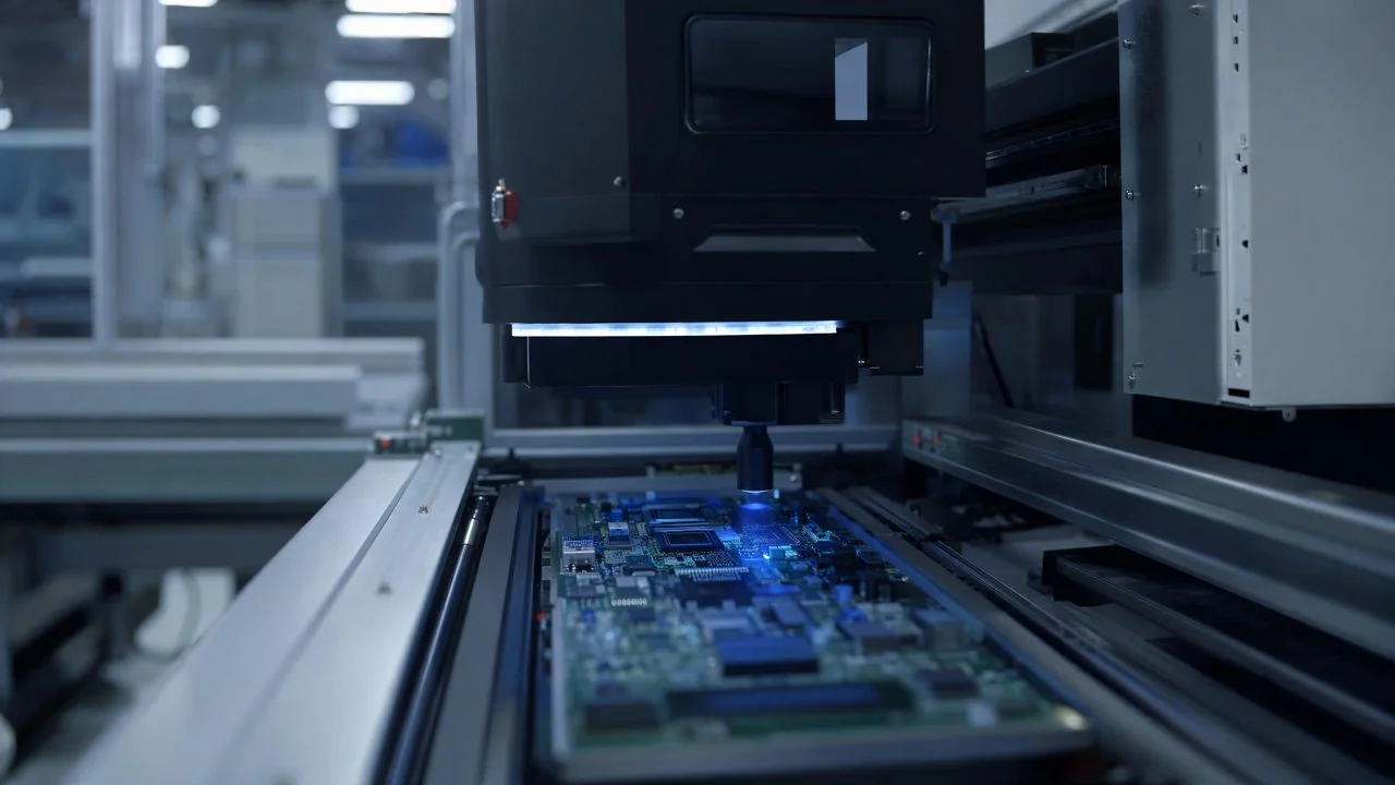
In the electronics/PCBA industry, the detection of hidden solder joints under BGA/QFN packages has always been a challenge. WeLinkirt's 3D ACI device provides an effective solution to this problem with its self-developed technology.
Industry background and user scenario: The electronics/PCBA industry is developing rapidly, with the integration and complexity of products continuously increasing. A well-known electronics manufacturing company's production line focuses on producing high-precision circuit boards, which involve a large number of chips in BGA/QFN packages. The hidden solder joints in these packages are the key objects for detection, as they directly affect the performance and stability of the circuit boards. In the production process, strict inspection of these hidden solder joints is required after the placement process to ensure that the product quality meets high standards.
Pain points: Why is this hurdle so hard to cross?
Multidimensional quantification of pain points: Previously, the company used traditional detection methods and faced many difficulties. The miss-detection rate was as high as 1.5%, which means that for every 1000 products produced, 15 products with hidden solder joint defects might flow into the market, bringing great quality risks. The false-alarm rate reached 20%. A large number of false-alarm messages required manual re-judgment, and the manual re-judgment working hours accumulated over 100 hours per month, which not only increased labor costs but also affected production efficiency. The change-over downtime was relatively long, taking 30 minutes each time, seriously affecting the flexibility of the production line and the production rhythm. In addition, due to insufficient detection accuracy, there was a certain compliance risk, which might lead to serious consequences such as product recalls, and the detection cost per unit was also relatively high.
Root cause analysis: From the process level, the hidden solder joints in BGA/QFN packages are located under the chips, and traditional 2D optical detection is difficult to directly observe, easily resulting in detection blind spots. In terms of imaging, 2D optical imaging can only provide planar information and cannot obtain the 3D morphology and height information of solder joints, making it difficult to accurately judge some minor defects and coplanarity problems. In terms of materials, the material and surface characteristics of solder joints will affect the reflection and absorption of light, resulting in unstable imaging quality. Considering the production rhythm, the high-speed operation of the production line requires the detection equipment to complete the detection task quickly and accurately, while traditional methods are difficult to balance detection speed and accuracy. Combining with the causal world model, traditional detection methods lack in-depth understanding and analysis of the causes of defects and cannot establish an effective causal relationship model, resulting in frequent miss-detection and false-alarm situations.
Technical principle
In-depth mechanism: The 3D ACI device of WeLinkirt uses a self-developed 3D camera. Through the structured light projection technology, a specific light pattern is projected onto the object to be measured, and then the camera captures the distortion information of the reflected light. Through the 3D morphology reconstruction algorithm, this distortion information is converted into 3D point-cloud data, thereby accurately restoring the 3D morphology of the solder joints. The device also uses 2D-3D fusion technology, combining the texture information of 2D images and the geometric information of 3D point clouds to improve the detection accuracy. In terms of algorithms, advanced deep learning algorithms are used to train a large number of solder joint samples, enabling the device to automatically identify different types of defect features.
Comparison with traditional methods: Compared with rule-based AOI, rule-based AOI mainly detects based on preset rules and thresholds and has difficulty accurately identifying complex and changeable solder joint defects. In contrast, the 3D ACI device can adaptively learn and identify various defects through deep learning algorithms, with higher detection accuracy. Compared with manual visual inspection, manual visual inspection is limited by human visual fatigue and subjective judgment, with low detection efficiency and high miss-detection rate. The 3D ACI device can quickly and accurately complete the detection task, greatly improving the detection efficiency and accuracy.
Typical application scenarios
- Detecting solder joint cold-soldering: The 3D point-cloud data is used to determine whether the height and shape of the solder joints meet the standards. The difficulty lies in that the features of cold-soldering may be relatively subtle, requiring high-precision 3D imaging and complex algorithms for accurate identification.
- Detecting coplanarity problems: The 3D morphology reconstruction technology is used to obtain the flatness information of the solder joints and determine whether there are coplanarity deviations. The difficulty lies in accurately measuring the flatness of tiny solder joints, which requires extremely high precision of the equipment.
- Detecting micron-level morphology defects: Such as tiny cracks and protrusions on the surface of solder joints, the 2D-3D fusion technology is used to comprehensively analyze the texture and geometric information to detect defects. The difficulty lies in that micron-level defects are not obvious in the image, requiring high-resolution imaging and powerful image-processing capabilities.
- Detecting porosity defects: The void information in the 3D point-cloud data is analyzed to identify porosity. The difficulty lies in that the size and shape of the pores vary, and the algorithm needs to be able to adaptively identify different types of pores.
Implementation case
Comparison before and after the implementation for the anonymous customer: After the well-known electronics manufacturing company introduced WeLinkirt's 3D ACI device, the implementation process was relatively smooth. The equipment supplier provided professional installation, debugging, and training services to ensure that the company's employees could operate the equipment proficiently. Before the implementation, the company's miss-detection rate was 1.5%, the false-alarm rate was 20%, and the change-over downtime was 30 minutes. After the implementation, the miss-detection rate was reduced to <0.1%, the false-alarm rate was reduced to 3%, and the change-over downtime was shortened to 5 minutes. These data indicate that the introduction of the device significantly improved the detection accuracy and the flexibility of the production line.
The application of the 3D ACI device provides strong support for electronics manufacturing companies to solve the problem of detecting hidden solder joints in BGA/QFN packages.
WeLinkirt's solution and product
Product capabilities and implementation methods: Centered on the 3D ACI device, WeLinkirt provides a end-to-end solution. In terms of modeling, using the DaoAI ACI OS, zero-code automatic programming can be completed for a good product in only 5 minutes. Combined with APDT positive-sample/few-sample learning (only 1-20 good samples are needed), an accurate detection model can be quickly established. In terms of change-over, the device has the ability of rapid change-over, and the change-over settings can be completed in 5 minutes to meet the rapid switching needs of the production line. In terms of deployment, it supports various deployment methods such as SDK / API / Docker and can achieve 100% local private deployment to ensure that the data does not leave the factory. At the same time, the device can be integrated with the company's existing production line to smoothly connect with the production process.
Quantitative results and business value: By introducing the 3D ACI device, the detection accuracy of the company has been greatly improved. The miss-detection rate has been reduced by more than 93%, greatly reducing the quality risks caused by defective products flowing into the market. The false-alarm rate has been reduced by 85%, reducing the manual re-judgment working hours and labor costs. The change-over downtime has been shortened by 83%, improving the flexibility and production efficiency of the production line, and the detection cost per unit has also been significantly reduced. In addition, the high-precision detection ability of the device helps the company meet more stringent industry compliance requirements and enhance its market competitiveness.
FAQ
What types of hidden solder joint defects can the 3D ACI device detect?
The 3D ACI device can detect cold-soldering, coplanarity problems, micron-level morphology defects, and porosity defects of hidden solder joints in BGA/QFN packages. Through the self-developed 3D camera and 2D-3D fusion technology, it can accurately identify different types of defects with high detection accuracy.
How long does it take for the device to complete a change-over?
WeLinkirt's 3D ACI device has the ability of rapid change-over and only takes 5 minutes to complete the change-over settings. This greatly shortens the downtime of the production line and improves production efficiency and flexibility.
How much can the detection cost be reduced by using this device?
Using this device can significantly reduce the detection cost. The false-alarm rate is reduced by 85%, which reduces the manual re-judgment working hours. The miss-detection rate is reduced by more than 93%, which reduces the quality risk cost. The shortening of the change-over downtime also improves production efficiency, comprehensively reducing the detection cost per unit.
Full solution for this scenario: Semiconductor / chips industry solutions
This article was generated by AI. Customer cases are simulated scenarios based on real product capabilities and figures are illustrative; see product pages for official benchmarks.