
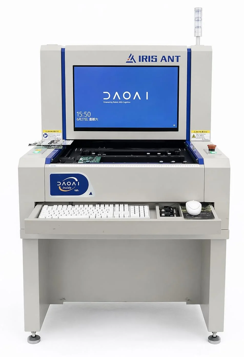
DaoAI 2D ACI equipment (high-resolution 2D imaging + deep learning secondary judgment, targeting surface/print/OCR/assembly defects, high-speed online full inspection, micron-level, semantic false positive filtering) leverages innovative zero-code rapid changeover capabilities to reduce SMT solder joint defect inspection changeover downtime from an average of 60 minutes with traditional AOI to under 5 minutes in high-mix low-volume electronic manufacturing, significantly boosting production line flexibility and overall equipment effectiveness (OEE).
In today's highly competitive electronics manufacturing industry, PCBA (Printed Circuit Board Assembly) is a core component whose quality directly determines the performance and reliability of end products. With shorter consumer electronics product lifecycles, growing demand for personalization, and the pursuit of customization and high reliability in industrial control and automotive electronics, High-Mix Low-Volume (HMLV) production has become the norm. Under this model, frequent changeovers on SMT (Surface Mount Technology) lines are an unavoidable challenge, especially in solder joint quality inspection. Traditional SMT solder joint defect detection, such as voids, bridges, and insufficient solder, demands extremely high precision and speed. Moreover, adjusting inspection programs during product model changes is often time-consuming and labor-intensive, severely impacting production line efficiency. DaoAI 2D ACI equipment precisely addresses this core pain point, providing an efficient and flexible solution for electronics manufacturers, ensuring solder joint inspection quality and production rhythm in complex manufacturing environments.
Pain Points: Why This Hurdle is Difficult to Overcome
SMT solder joint inspection in high-mix low-volume production faces multiple challenges. Firstly, **long changeover downtime**. Traditional rule-based AOI (Automated Optical Inspection) systems require engineers to manually adjust numerous parameters and write complex inspection rules during product model changes, with a single changeover typically taking 45-90 minutes. Production line data from a mid-sized electronics manufacturer showed an average changeover time of up to 60 minutes. Secondly, the **dilemma of balancing false positives and false negatives**. For micron-level defects like voids, subtle bridges, and irregular insufficient solder, traditional AOI rules struggle to cover all variations, making it difficult to reduce false negatives below <0.5%. To lower false negatives, rules must be relaxed, leading to higher false positives; actual measurements on one production line showed false positives often around 3%, resulting in numerous good products being misidentified and increasing the burden of manual re-inspection. Thirdly, **inefficient and subjective manual re-inspection**. Due to false positives, a significant amount of manual secondary re-inspection is required in downstream processes. At a mid-sized electronics manufacturer, manual re-inspection accounted for up to 15% of labor hours, which is not only costly but also suffers from inconsistent judgment standards among different operators, making quality consistency difficult to guarantee. Furthermore, the growing industry demand for generalization capabilities in defect detection, similar to research on strategies for balancing generalization and precision in industrial defect detection using SAM zero-shot segmentation technology, also reflects the lack of adaptability of traditional solutions when facing unknown or few-shot defects.
The root cause of these pain points lies in the inherent difficulty of SMT solder joint inspection and the limitations of traditional technologies. Solder joint morphology is complex and varied, influenced by factors such as solder paste printing, reflow soldering temperature profiles, and component lead shapes; even the same type of defect can exhibit different visual characteristics. Traditional AOI relies on fixed rules set by engineer experience, which struggles to adapt to this high-dimensional variability. When product models are frequently changed, the PCBA layout, component types, and pad sizes of new and old models may all change, rendering previous rules ineffective and requiring complete re-configuration or significant modifications. This hard-coded, rule-based approach proves inadequate for the flexible demands of high-mix low-volume production, making changeover programming a bottleneck that severely restricts overall line efficiency and responsiveness.
Technical Principles
DaoAI 2D ACI equipment fundamentally solves SMT solder joint defect detection challenges by integrating high-resolution 2D imaging technology with advanced deep learning secondary judgment mechanisms. Its core lies in the DaoAI ACI OS operating system, which incorporates a visual foundation model with powerful feature recognition capabilities. For solder joint defect detection, the DaoAI 2D ACI equipment first uses high-resolution industrial cameras to capture clear images of PCBA boards, capturing detailed solder joint morphology. These image data are then fed into a deep learning model for initial analysis. Unlike traditional AOI, which relies on manually set thresholds and geometric rules, DaoAI 2D ACI employs APDT positive/few-shot learning (1–20 good samples) training. With only a small number of good samples, the system can automatically program within 5 minutes, quickly learning and understanding the visual characteristics of 'normal' solder joints. When an area that does not match the characteristics of good samples is detected, the system flags it as a potential defect.
Furthermore, DaoAI 2D ACI equipment introduces deep learning secondary judgment and semantic false positive filtering mechanisms. Traditional methods often output results directly after initial judgment, leading to higher false positive rates. DaoAI 2D ACI's secondary judgment, using deeper semantic understanding, re-analyzes initially identified defects, combining contextual information and structural features of solder joints to effectively distinguish true defects from normal variations in the production process (e.g., solder surface texture, slight reflections). This mechanism enables DaoAI 2D ACI to reduce SMT solder joint inspection false positive rates by over −80% in actual applications, while keeping false negatives below <0.4%. Compared to the rule limitations of traditional AOI and the subjectivity of manual visual inspection, DaoAI 2D ACI demonstrates superior engineering depth and robustness, especially when facing frequent changeover demands in high-mix low-volume production. Its "zero-code rapid changeover" capability is a significant advantage, eliminating the need for complex parameter adjustments; engineers can simply operate to switch inspection programs for new products, reducing changeover time from tens of minutes to just minutes.
Typical Application Scenarios
- **SMT Void Detection**: DaoAI 2D ACI can precisely identify voids or air bubbles inside or at the edges of solder joints, as well as voids caused by poor wetting between solder and pads or leads. The challenge lies in the diverse forms of voids and their sometimes inconspicuous surface features, requiring high-resolution imaging and the fine feature extraction capabilities of deep learning.
- **SMT Solder Bridge (Short Circuit) Detection**: For tiny solder bridges between adjacent pads or leads, DaoAI 2D ACI can achieve micron-level precision detection. The difficulty is that bridges can be very subtle and influenced by lighting, angles, etc., making them easily missed by traditional methods or misidentified as normal solder splashes.
- **SMT Insufficient Solder/Open Circuit Detection**: Detects insufficient solder volume in solder joints or completely missing solder leading to open circuits. The challenge involves judging the degree of insufficient solder and distinguishing it from normal variations in solder joint top flatness. DaoAI 2D ACI accurately determines if solder volume meets standards by learning the 3D contour characteristics of a large number of good solder joints.
- **Component Misalignment/Skew Detection**: Beyond the solder joints themselves, DaoAI 2D ACI can also detect if components are correctly positioned on pads after SMT placement, identifying issues like skew, tombstoning, or side-standing. The difficulty arises from small component spacing in high-density assembly, requiring precise localization and dimension measurement.
- **Character OCR and Barcode Recognition**: On PCBA boards, DaoAI 2D ACI can perform high-speed OCR recognition and verification of silkscreen characters, component markings, QR codes/barcodes to ensure information accuracy. The challenge lies in inconsistent character print quality and complex backgrounds that can interfere with recognition; the system effectively overcomes these challenges through deep learning models.
Deployment Case Study
A mid-sized electronics manufacturer in South China, primarily undertaking OEM/ODM business for industrial control boards and customized consumer electronics, is characterized by high-mix, low-volume, and frequent changeovers. Before introducing DaoAI 2D ACI equipment, the factory used traditional AOI equipment for SMT solder joint inspection. Production line data indicated that due to frequent product model changes (at least 3-5 times per week), each changeover programming and debugging averaged 60 minutes, leading to annual losses of millions of RMB from changeover downtime. Furthermore, the traditional AOI's false positive rate remained high, with an average measured false positive rate of about 3%, requiring 3-4 skilled workers to perform manual re-inspection for up to 4 hours daily, which not only incurred significant labor costs but also resulted in re-inspection results being heavily influenced by subjective factors.
To address these pain points, the factory introduced DaoAI 2D ACI equipment. During the deployment process, the DaoAI team first assisted the client in collecting a small number of good samples (only 10-20 images per model). Utilizing the APDT few-shot learning function built into the DaoAI ACI OS operating system, the automatic programming of the inspection program for the first new product model was completed within 5 minutes. After a two-week trial run and fine-tuning, the system operated stably and achieved significant results. After deployment, the factory's SMT solder joint inspection changeover time was reduced to under 5 minutes, with an actual average of just 3.5 minutes, significantly enhancing production line flexibility and OEE. Concurrently, the deep learning secondary judgment function of DaoAI 2D ACI effectively reduced the false positive rate, decreasing it from 3% to <0.6%, which reduced manual re-inspection workload by over 70% and freed up substantial human resources. Additionally, in this case, the system's detection rate for core defects like voids, bridges, and insufficient solder increased to over 99.6%, far exceeding the performance of traditional AOI.
DaoAI 2D ACI not only achieved high-precision solder joint defect detection but also, with its zero-code rapid changeover capability, completely transformed our efficiency bottleneck in high-mix low-volume production, bringing tangible cost reduction and efficiency gains.
DaoAI Solution and Products
The core of the DaoAI 2D ACI solution lies in its innovative DaoAI ACI OS operating system and high-resolution 2D imaging hardware. In SMT solder joint defect detection scenarios, the deployment process of DaoAI 2D ACI equipment is highly simplified. Customers do not need professional AI programming knowledge; they simply import a small number of good product images (typically 1-20) through a graphical interface, and the system leverages the APDT few-shot learning function to automatically generate efficient and robust inspection models within minutes. This "zero-code" modeling approach greatly shortens the model development cycle and changeover time, making frequent product switches in high-mix low-volume production no longer an efficiency bottleneck. DaoAI 2D ACI supports 100% local private deployment, ensuring data never leaves the premises, guaranteeing customer data security and production autonomy. Simultaneously, its open SDK/API interfaces allow for easy integration with existing MES/ERP systems, enabling closed-loop management and traceability of production data.
The semantic false positive filtering function of DaoAI 2D ACI equipment is one of its key advantages distinguishing it from traditional solutions. By performing deep semantic analysis of defect areas, the system can effectively differentiate true defects that impact product quality from harmless surface texture variations, thereby significantly reducing false positive rates and the workload of manual re-inspection. In the actual application at a mid-sized electronics manufacturer, the DaoAI 2D ACI solution successfully reduced SMT solder joint inspection changeover time to under 5 minutes, decreased false positive rates by over −80%, and ensured a detection rate of over 99.6% for critical defects. These quantified achievements directly translate into significant business value: improved line OEE, reduced labor costs, shortened time-to-market, and ultimately enhanced the client's competitiveness in the HMLV market. DaoAI 2D ACI is not merely an inspection device; it is a crucial tool enabling electronics manufacturers to achieve intelligent and flexible production.
FAQ
How does DaoAI 2D ACI equipment achieve "zero-code rapid changeover" for SMT solder joint inspection?
DaoAI 2D ACI equipment achieves this through the visual foundation model and APDT few-shot learning technology embedded in its DaoAI ACI OS operating system. Users only need to provide 1-20 images of good products, and the system automatically learns product features and generates an inspection model within minutes, eliminating the need for complex rule or code writing, thus significantly reducing changeover time.
How are the deployment costs and payback period of the DaoAI 2D ACI solution evaluated?
The deployment cost of the DaoAI 2D ACI solution is influenced by factors such as equipment configuration, integration requirements, and production line scale. By significantly reducing changeover downtime, lowering manual re-inspection costs, and improving product quality, customers typically achieve ROI within 6-18 months. For specific quotes and payback period assessments, we recommend contacting our sales team for a customized solution.
What unique advantages does DaoAI 2D ACI equipment offer when detecting SMT solder joint bridging?
When detecting SMT solder joint bridging, DaoAI 2D ACI equipment utilizes high-resolution 2D imaging to capture micron-level details. Through deep learning secondary judgment and semantic false positive filtering, it precisely identifies minute solder bridges. Its learning capability effectively distinguishes subtle bridging from normal solder splashes, significantly reducing false negatives and false positives, outperforming traditional rule-based AOI.
Full solution for this scenario: 2D ACI Equipment industry solutions
This article was generated by AI. Customer cases are simulated scenarios based on real product capabilities and figures are illustrative; see product pages for official benchmarks.