
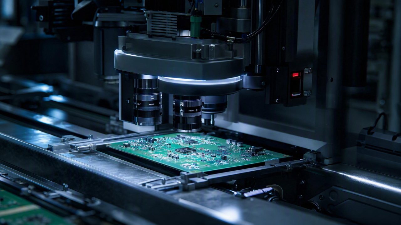
In electronics manufacturing, particularly on PCBA (Printed Circuit Board Assembly) production lines, the quality of SMT (Surface Mount Technology) solder joints directly dictates the reliability and performance of the final product. DaoAI 2D AI AOI equipment (high-resolution 2D imaging + deep learning secondary judgment, targeting planar defects like surface imperfections, printing errors, OCR characters, and assembly omissions, with high-speed inline full inspection, micron-level precision, and semantic false positive filtering) successfully boosted the PCBA SMT solder joint inspection line throughput for a leading electronics manufacturer from 280ms to 180ms, ensuring 100% full inspection coverage for micron-level defects by integrating high-speed, high-resolution imaging with semantic false positive filtering technology. This not only significantly improved production efficiency but also substantially reduced rework and customer complaint risks stemming from solder joint defects.
DaoAI 2D AI AOI equipment (high-resolution 2D imaging + deep learning secondary judgment, targeting planar defects like surface imperfections, printing errors, OCR characters, and assembly omissions, with high-speed inline full inspection, micron-level precision, and semantic false positive filtering) successfully boosted the PCBA SMT solder joint inspection line throughput for a leading electronics manufacturer from 280ms to 180ms, ensuring 100% full inspection coverage for micron-level defects by integrating high-speed, high-resolution imaging with semantic false positive filtering technology. In the field of electronics manufacturing, the quality of SMT (Surface Mount Technology) solder joints on PCBAs is paramount. With the increasing demand for miniaturization and high integration in consumer electronics, automotive electronics, and other products, solder joint density on PCBAs is growing, and sizes are shrinking, posing stringent challenges to inspection speed and accuracy. Traditional inspection methods often struggle to keep pace with modern production line takt times, leading to prominent issues of missed detections or false positives. This case focuses on the inline full inspection of SMT solder joints (cold solder, bridging, insufficient solder), where timely detection and correction of these defects are crucial for ensuring product reliability.
Pain Points: Why This Hurdle is Difficult to Overcome
High-speed PCBA production lines face multiple challenges in SMT solder joint inspection. Firstly, there's the pressure of production takt time; a leading electronics manufacturer required single board inspection within 200ms, whereas traditional rule-based AOI averaged 280ms for complex board types, creating a production bottleneck and preventing 100% inline full inspection. Secondly, high false positive rates: traditional rule-based AOI is highly prone to false positives due to solder joint luster, uneven reflection, or slight shadows, leading to a massive workload for manual re-inspection. A measured false positive rate of up to 18% significantly slowed overall production efficiency and increased manual re-inspection labor by 30%. Thirdly, the risk of missed minute defects: defects like cold solder, insufficient solder, or slight bridging typically range from tens to hundreds of microns and can be hidden under component leads or on highly reflective surfaces. Traditional AOI struggles to consistently detect these, resulting in approximately a 0.8% missed detection rate on this client's line. Furthermore, light and material interference in reflective surface defect detection is a common technical challenge, as solder joint surfaces can exhibit specular or diffuse reflection at different angles, leading to unstable image features and further increasing the difficulty of false positives and missed detections.
The root cause of these pain points lies in the physical characteristics of SMT solder joints and the limitations of traditional inspection methods. Solder joints are metallic, often have uneven surfaces, and can exhibit varying degrees of luster, color, and shape after reflow soldering. Traditional rule-based AOI primarily relies on predefined geometric shapes, grayscale thresholds, and other rules, making it less robust to lighting variations, background noise, and subtle differences in solder joint morphology. When dealing with reflective surfaces, changes in incident and exit light angles significantly impact image acquisition, creating “false defects” or “missed defects.” While manual visual inspection can handle complex situations, it is slow, prone to fatigue, lacks consistency, and cannot meet the demands of high takt times and 100% full inspection. These factors collectively constitute a major obstacle to high-speed, high-precision full inspection of PCBA solder joints.
Technical Principles
DaoAI 2D AI AOI equipment fundamentally resolves the aforementioned challenges by combining high-resolution 2D imaging with advanced deep learning secondary judgment technology. First, at the imaging end, DaoAI employs multi-angle annular lighting and high-resolution industrial cameras capable of capturing subtle features of solder joints under various lighting conditions, effectively suppressing reflection interference. Techniques like polarized light or multispectral imaging can further enhance the contrast between solder joints and the background, distinguishing reflective properties of different materials, thereby providing high-quality, stable data for subsequent AI analysis during the image acquisition phase. Second, the core lies in its integrated DaoAI AI AOI software system, which leverages the feature recognition capabilities of visual foundation models. This system learns complex features such as normal morphology, color, and luster of solder joints from a large volume of good product data, building a high-dimensional “good product” model. For suspected defect areas, the system performs deep learning secondary judgment, using convolutional neural networks (CNNs) for pixel-level semantic understanding and classification of image regions, distinguishing true defects from background noise, lighting artifacts, and other interferences, thus achieving semantic false positive filtering. This semantic understanding-based judgment allows DaoAI 2D AI AOI equipment to far surpass traditional AOI in detecting defects on reflective surfaces.
Compared to traditional rule-based AOI, the advantage of DaoAI 2D AI AOI equipment lies in its powerful generalization and adaptability. Traditional AOI requires engineers to manually write complex rules, demanding significant time for rule adjustment with each new product or process change. It also has low sensitivity to subtle image variations and is susceptible to ambient light, component tolerances, etc. In contrast, the DaoAI 2D AI AOI solution, through APDT positive/few-shot learning technology, can quickly train high-precision detection models with just 1–20 good product images, significantly reducing changeover time. For instance, in one case, PCBA changeover time was reduced from a traditional 2 hours to 5 minutes. Furthermore, its deep learning model can identify and learn the subtle visual cues that human experts rely on during re-inspection, reducing the false positive rate from the traditional 18% to below 4%, significantly improving inspection efficiency and accuracy. In practical applications, the DaoAI 2D AI AOI equipment can consistently achieve a 99.7% detection rate for micron-level solder joint defects at a single board inspection takt time of 180ms, far exceeding the performance limits of traditional AOI.
Typical Application Scenarios
- **SMT Solder Joint Defect Detection:** This is the most critical application, targeting inline full inspection of various solder joint morphology anomalies such as cold solder (collapsed solder, poor wetting), bridging (solder bridging), insufficient solder, excessive solder, tombstoning, and misalignment. The challenge lies in tiny solder joint sizes, diverse shapes, and complex surface reflections. DaoAI 2D AI AOI precisely identifies these micron-level defects through multi-angle imaging and deep learning models.
- **Component Missing, Misalignment, and Polarity Detection:** Correct component placement is crucial in PCBA assembly. The equipment can high-speed detect missing resistors, capacitors, ICs, etc., misalignment from pads, and reverse mounting of polarized components. The difficulty lies in the wide variety of component types, large size differences, and indistinct identification features. DaoAI 2D AI AOI, with its powerful feature learning capabilities, consistently distinguishes these.
- **PCB Surface Scratch and Contamination Detection:** PCB substrates may exhibit surface defects such as scratches, foreign objects, or oil stains during production and transportation. While these defects do not directly affect electrical performance, they impact product appearance and long-term reliability. DaoAI 2D AI AOI equipment's high-resolution imaging and fine defect recognition capabilities effectively detect these minute surface imperfections.
- **Character OCR/OVC Detection:** PCBAs often have batch numbers, model numbers, production dates, and other characters for traceability and management. The equipment can perform character recognition (OCR) and verification (OVC), detecting issues like blurry, missing, or misprinted characters. The challenge lies in the wide variation of fonts, sizes, and print quality. The DaoAI AI AOI software system ensures high accuracy through specialized character recognition models.
Case Study
A leading Tier-1 electronics product supplier had extremely high demands for inspection efficiency and accuracy on its PCBA production line. Before introducing DaoAI 2D AI AOI equipment, the line primarily relied on traditional rule-based AOI for initial inspection, supplemented by extensive manual re-inspection. The traditional AOI's single board inspection takt time was 280ms, unable to meet the growing production capacity demands, often creating production bottlenecks. More critically, the traditional AOI's false positive rate was as high as 18%, requiring 4 skilled workers to spend 8 hours daily on manual re-inspection, which not only increased labor costs but also introduced inconsistencies due to human judgment. Furthermore, tiny cold solder and bridging defects still had a missed detection rate of about 0.8%, posing risks to downstream assembly and end-product reliability. Facing these challenges, the supplier decided to introduce the DaoAI 2D AI AOI solution.
After one month of on-site integration and model training, the DaoAI 2D AI AOI equipment was successfully deployed. Post-deployment, production line data showed that the equipment's single board inspection takt time was stably controlled at 180ms, an improvement of 35%. Concurrently, thanks to the powerful semantic false positive filtering capability of the DaoAI AI AOI software system, the false positive rate dramatically decreased from 18% to below 4%, a reduction of 78%. This significantly reduced the manual re-inspection workload, requiring only 1 operator for minimal auxiliary review per shift, saving substantial human resources. Most importantly, the DaoAI 2D AI AOI equipment's detection rate for micron-level SMT solder joint defects like cold solder, bridging, and insufficient solder increased to over 99.7%, with a missed detection rate reduced to below 0.3%, effectively preventing critical defects from reaching downstream processes. The client's production director stated that DaoAI 2D AI AOI not only resolved production line takt time bottlenecks but also significantly improved product quality and customer satisfaction.
“The deployment of DaoAI 2D AI AOI has completely transformed our PCBA solder joint inspection process. It not only eliminated production line takt time bottlenecks but, more importantly, by drastically reducing false positives, our inspection team can now focus on higher-value tasks, and product quality has reached unprecedented levels.”
DaoAI Solutions and Products
The DaoAI 2D AI AOI solution, centered around its core 2D AI AOI equipment, provides a comprehensive PCBA SMT solder joint inspection solution. This equipment integrates high-resolution industrial cameras, a multi-angle lighting system, and a high-performance edge computing unit, ensuring high-speed and high-quality image acquisition. Its core capabilities are powered by the DaoAI AI AOI software system, which utilizes advanced visual foundation models. Through APDT positive/few-shot learning technology, it requires only 1–20 good product samples to complete model training, enabling 0-code automated programming. This significantly simplifies the complexity of model deployment and maintenance. For reflective surface defects, the deep learning secondary judgment module of the DaoAI 2D AI AOI equipment performs fine-grained semantic analysis on suspected defects, effectively distinguishing true defects from artifacts caused by lighting and material, thereby achieving over 95% semantic false positive filtering and keeping the false positive rate at an extremely low level. For deployment, DaoAI offers various integration methods such as SDK/API/Docker, supporting 100% local private deployment to ensure customer data security. For different production line environments and customer needs, the DaoAI engineering team provides end-to-end services from preliminary assessment, solution design, equipment integration, to post-maintenance, ensuring smooth implementation and long-term stable operation of the solution.
In actual projects, the DaoAI 2D AI AOI equipment has demonstrated exceptional performance. The solution boosted production line takt time by 35%, from 280ms to 180ms, significantly enhancing production efficiency. Concurrently, combined with the semantic false positive filtering capabilities of the DaoAI AI AOI software system, manual re-inspection labor hours were reduced by 75%, greatly optimizing human resource allocation. The equipment achieved a detection rate of over 99.7% for micron-level defects such as cold solder, bridging, and insufficient solder in PCBA SMT solder joint inspection, ensuring the stability and reliability of product quality. DaoAI is committed to providing efficient, precise, and user-friendly intelligent vision inspection solutions to help electronic manufacturing enterprises achieve digital transformation and intelligent upgrades.
FAQ
How does DaoAI 2D AI AOI equipment address lighting interference on reflective solder joint surfaces?
DaoAI 2D AI AOI equipment utilizes multi-angle annular lighting, along with polarized or multispectral imaging technology, to capture subtle features of solder joints under various lighting conditions, effectively suppressing reflection interference. Combined with deep learning models for semantic understanding of images, it distinguishes true defects from lighting artifacts, thereby overcoming technical challenges in reflective surface defect detection.
What are the advantages of this equipment over traditional rule-based AOI in terms of production takt time and false positive rate?
DaoAI 2D AI AOI equipment optimizes imaging and deep learning secondary judgment, boosting single board inspection takt time from traditional AOI's 280ms to 180ms, an improvement of 35%. Concurrently, its semantic false positive filtering capability reduces the false positive rate from 18% to below 4%, a reduction of 78%, significantly cutting down manual re-inspection workload.
What is the approximate cost and timeline for deploying the DaoAI 2D AI AOI solution?
The cost of the DaoAI 2D AI AOI solution is influenced by factors such as equipment configuration, production line scale, integration complexity, and customization requirements. Typically, the timeline from needs assessment to equipment go-live is about 1–3 months. We provide customized quotes; please contact our sales team for a detailed proposal and budget estimation.
This article was generated by AI. Customer cases are simulated scenarios based on real product capabilities and figures are illustrative; see product pages for official benchmarks.