
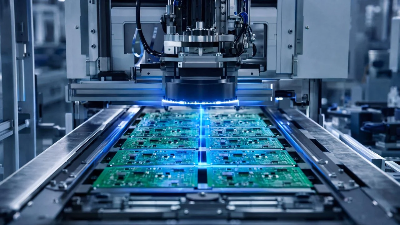
Against a backdrop of increasing global supply chain uncertainties and accelerating intelligent manufacturing transformation, electronics/PCBA manufacturers face unprecedented challenges and opportunities. Particularly on SMT (Surface Mount Technology) production lines, solder joint quality is crucial for product reliability. DaoAI 2D ACI equipment (high-resolution 2D imaging + deep learning secondary judgment, targeting planar defects like surface/print/OCR/assembly omissions, high-speed inline full inspection, micron-level, semantic false positive filtering), by integrating domestic AI computing power with edge control, precisely identifies SMT solder joint defects such as cold solder, bridging, and insufficient solder. This has reduced false positive rates from traditional manual re-inspection by 63%, effectively enhancing PCBA production quality control and efficiency, and significantly bolstering the resilience of intelligent manufacturing lines.
DaoAI 2D ACI equipment (high-resolution 2D imaging + deep learning secondary judgment, targeting planar defects like surface/print/OCR/assembly omissions, high-speed inline full inspection, micron-level, semantic false positive filtering) integrates high-precision 2D imaging with advanced deep learning algorithms. In SMT solder joint inspection scenarios, it has reduced false positive rates from traditional manual re-inspection by 63% and increased solder joint defect detection rates to 99.4%, significantly elevating PCBA manufacturing quality control and production efficiency. In the electronics/PCBA industry, reflow soldering after SMT placement is a core process, and solder joint quality directly impacts product electrical performance and long-term reliability. As electronic products trend towards miniaturization and higher integration, PCBA component density continuously increases, and pad spacing shrinks, posing extremely high demands on solder joint inspection. The client in this case is a Tier-1 supplier specializing in high-end industrial control modules and automotive electronics, whose products demand stringent reliability; any minor solder joint defect could lead to severe consequences. Their main challenge was how to accurately and efficiently detect micron-level planar solder joint defects such as cold solder, bridging, and insufficient solder in high-throughput production, while reducing false positives and alleviating the pressure of manual re-inspection.
Pain Points: Why This Hurdle Was Difficult to Overcome
This leading manufacturer faced multiple challenges in SMT solder joint inspection: Firstly, the false positive rate of manual visual inspection and traditional rule-based AOI was as high as 5%~8%, leading to a large number of good products being misjudged, requiring significant manual re-inspection hours—at least 4 skilled workers dedicated daily, severely dragging down production line efficiency. Secondly, the traditional methods still had a false negative rate of 0.6%~1% for tiny cold solder joints, hidden bridging (e.g., BGA bottom edge bridging), or subtle insufficient solder, which was an unacceptable risk for their high-reliability industrial-grade products, potentially leading to mass recalls. Furthermore, when changing models for new products, traditional AOI required several hours or even half a day for program adjustments and parameter optimization, seriously impacting production line flexibility and utilization. The root cause of these dilemmas is that traditional rule-based AOI relies on engineers manually writing complex rules for geometric shapes, grayscale thresholds, etc., which struggles to adapt to the diversity and complexity of solder joint morphology, especially in dense component areas where solder joints may be affected by surrounding shadows or reflections, leading to misjudgments. Simultaneously, with the trend of integrating domestic AI computing power with industrial controllers, traditional AOI lacks deep integration with edge AI computing, making it unable to achieve real-time, high-precision intelligent decision-making, encountering bottlenecks in processing massive image data, leading to a “lack of power” in complex defect recognition and difficulty in improving intelligent manufacturing resilience.
Moreover, the inherent instability of the reflow soldering process, fluctuations in solder paste printing quality, and component lead coplanarity issues can all create elusive defect types on the solder joint surface. For instance, cold solder might manifest as a rough surface, tiny cracks, or poor wetting; bridging could be a minuscule solder bridge between two pads; and insufficient solder might appear as inadequate solder volume or an abnormal wetting angle. These defects often present as subtle texture, brightness, or morphological changes in 2D images, making them extremely difficult for human eyes and fixed-rule algorithms to distinguish or overlook, especially on high-throughput production lines, where operator fatigue further escalates the risk of missed detections.
Technical Principles
The core of the DaoAI 2D ACI equipment lies in its “high-resolution 2D imaging + deep learning secondary judgment” technical architecture. First, the equipment utilizes industrial-grade high-resolution cameras and a customized multi-angle annular lighting system to capture multi-directional, high-definition 2D images of PCBA solder joints, obtaining rich optical feature information. This image data contains crucial information about solder joint shape, texture, brightness, and color, providing high-quality input for subsequent AI analysis. Second, the acquired image data is fed into an edge AI controller equipped with the DaoAI ACI OS. This system incorporates deep learning algorithms based on visual foundation models, capable of autonomously learning normal and abnormal patterns of solder joints from massive datasets. Unlike traditional rule-based AOI that relies on predefined thresholds, our deep learning model employs an APDT positive/few-shot learning mechanism, requiring only 1–20 good product images to quickly build a feature model for normal solder joints. When an anomaly is detected, the model performs deep feature extraction and matching to identify specific defect types such as cold solder, bridging, or insufficient solder. More importantly, the system integrates a semantic false positive filtering function, which can understand the “semantic” context of defects in the image, for example, distinguishing between normal solder overflow at the pad edge and actual bridging, or between component edge shadows and cold solder, thereby significantly reducing false positive rates. This mechanism, combining high-precision imaging with intelligent deep learning decision-making, enables the equipment to handle complex and varied defects that traditional methods struggle with, achieving micron-level precise inspection while ensuring real-time high-performance computing at the edge, supported by domestic AI computing power.
Compared to traditional rule-based AOI, DaoAI 2D ACI demonstrates significant advantages in several aspects: First, stronger adaptability—traditional AOI requires re-writing rules when encountering new products or process changes, which is time-consuming and labor-intensive, whereas ACI can quickly adapt to new solder joint morphologies and background changes through learning, without extensive manual adjustments. Second, higher recognition accuracy—deep learning models can capture subtle defect features that are difficult for human eyes and rules to detect, such as internal voids or tiny cracks in solder joints, significantly reducing false negatives. Third, lower false positive rates—the semantic false positive filtering mechanism effectively avoids misjudgments caused by lighting variations, component tolerances, or background noise, greatly reducing the workload of manual re-inspection. Fourth, simpler programming—one good product can be programmed automatically in 5 minutes with 0 code, greatly shortening changeover time and improving production line flexibility. Compared to manual visual inspection, ACI provides 100% inline full inspection capability, avoiding issues such as human eye fatigue, strong subjectivity, and low efficiency, while ensuring traceability of inspection results for consistent and objective quality control.
Typical Application Scenarios
- **SMT Solder Joint Cold Solder Detection:** After reflow soldering, inspect whether the solder joint surface exhibits poor wetting, tiny cracks, voids, or incomplete filling due to insufficient solder. The difficulty lies in the diverse forms of cold solder, which can be confused with normal solder joint textures; AI learns from a large number of cold solder samples to identify its subtle features.
- **SMT Solder Joint Bridging Detection:** Identify whether unintended solder bridges have formed between adjacent pads or pins. As component spacing shrinks, bridging can be extremely subtle and easily missed by traditional methods. AI can precisely distinguish between normal pad spacing and abnormal solder bridges, especially advantageous for hidden bridging (e.g., at QFN/BGA bottom edges).
- **SMT Solder Joint Insufficient Solder Detection:** Evaluate whether the solder joint volume is adequate and the wetting angle meets standards, preventing poor electrical connections due to insufficient solder. The challenge is quantifying solder joint volume and judging edges; AI accurately identifies insufficient solder defects by analyzing solder joint contours and grayscale information.
- **SMT Solder Joint Excessive Solder/Solder Blob Detection:** Identify solder joints with excessive solder leading to excessive height or irregular accumulation, which may cause short circuits or mechanical interference. AI models can learn the normal height and morphological distribution of solder joints to effectively detect abnormal solder blobs.
- **SMT Component Misalignment/Missing Detection:** Simultaneously with solder joint inspection, extend to identify whether components are misaligned, rotated, or completely missing after placement. This requires AI to have the ability to recognize the component body and correlate it with solder joint positions to ensure overall assembly quality.
Implementation Case Study
A leading Tier-1 supplier of industrial control and automotive electronics, with SMT production lines in East China, had long faced challenges in solder joint defect inspection. Their existing traditional rule-based AOI system struggled to reduce the false negative rate for complex solder joint defects (such as micron-level cold solder, hidden bridging) below 0.5%, while the false positive rate remained high, requiring 4 experienced engineers to conduct manual re-inspection for up to 6 hours daily, leading to high labor costs and low efficiency. Furthermore, new product changeovers required at least 2 hours for program adjustments, severely impacting the flexibility of production line switching. After the client introduced DaoAI 2D ACI equipment, we first conducted on-site data collection and model training. Utilizing the APDT few-shot learning capability of the DaoAI ACI OS, a model for the first product was trained in just 20 minutes using only 15 good product images. After deployment, the equipment smoothly integrated with the production line's MES system, achieving high-speed inline full inspection. Following a one-month trial run and optimization, results showed that the solder joint defect detection rate stabilized at 99.4%, with the false negative rate reduced to <0.6%. Especially for cold solder and hidden bridging, which were difficult for traditional AOI to identify, the detection capability significantly improved. Concurrently, thanks to semantic false positive filtering, the false positive rate for manual re-inspection dropped from the original 7.8% to 2.9%, reducing manual re-inspection hours by 63%. Now, only 1 engineer is needed for approximately 2 hours of spot checks and confirmation daily, greatly freeing up manpower. New product changeover time was also reduced from the original 2 hours to less than 5 minutes, significantly enhancing production line flexibility and utilization. The client highly praised the practical effectiveness of DaoAI 2D ACI equipment in improving product quality, reducing operating costs, and enhancing intelligent manufacturing resilience.
“DaoAI 2D ACI not only solved our long-standing challenges of solder joint missed detections and false positives, but more importantly, it brought AI intelligent decision-making to the edge of the production line, giving us unprecedented control over product quality.”
The figures above are a typically achievable range in anonymized industry scenarios — a different line or a different batch of parts will move the result either way; on-site measurement governs.
DaoAI Solution and Products
The core offering provided by DaoAI to this client was the 2D ACI equipment, which is powered by our independently developed DaoAI ACI OS. This system, centered on a visual foundation model, possesses powerful feature recognition capabilities, enabling 0-code automatic programming for one good product in 5 minutes, greatly simplifying model deployment and changeover processes. Through APDT positive/few-shot learning, clients only need to provide a small number of good product images, and the system can quickly establish high-precision inspection models, eliminating the need for a large number of defect samples and solving the problem of scarce defect data. The semantic false positive filtering function is another major highlight; it can deeply understand image content, effectively distinguish between real defects and background interference, thereby controlling the false positive rate to a very low level. In terms of deployment, our solution supports 100% local privatization, with all data remaining on-site, fully ensuring client data security and privacy. Additionally, we briefly mention that by leveraging the DaoAI World universal model as a unified foundation, future capabilities include cross-scenario generalization and continuous learning from production line feedback, constantly optimizing inspection models to adapt to more complex manufacturing demands. In this case, the 2D ACI equipment interacted with the client's existing MES system via standard interfaces, achieving real-time upload of inspection results and defect traceability, ensuring transparency and controllability of the production process.
The DaoAI 2D ACI equipment is not limited to solder joint inspection; its generalization capability allows it to cover various planar defect detection needs in PCBA production. For example, it can be used to detect printing defects such as solder paste volume, offset, or collapse after solder paste printing; assembly defects like component misalignment, absence, or reverse polarity after component placement; and surface defects such as board scratches, contamination, or character OCR recognition. Its high-speed inline full inspection capability ensures comprehensive and meticulous quality control for every product without affecting the production line's takt time. Through deep integration with domestic AI computing power (such as Kunlunxin Technology's edge AI controllers), our equipment achieves efficient inference at the edge, guaranteeing real-time data processing and decision-making, thereby enhancing the resilience of the entire intelligent manufacturing system. This integrated hardware-software, deep learning-driven inspection solution provides electronic manufacturing enterprises with a powerful tool to address complex production challenges, helping them maintain a leading position in fierce market competition.
FAQ
How does DaoAI 2D ACI equipment address the high false positive rate issue of traditional AOI?
Our 2D ACI equipment integrates a semantic false positive filtering function. This function, based on deep learning models, understands the 'semantic' context of defects in images, distinguishing true defects from disturbances caused by lighting, component tolerances, or background noise, thereby significantly reducing false positive rates and the workload of manual re-inspection.
What specific defect types can this equipment identify in SMT solder joint inspection?
DaoAI 2D ACI equipment can precisely identify common planar defects in SMT solder joints such as cold solder, bridging, insufficient solder, and excessive solder/solder blobs. Additionally, its generalization capability supports extended detection of component misalignment, absence, reverse polarity, as well as board scratches and contamination, providing comprehensive quality control.
How does 2D ACI achieve rapid changeover and model training?
Our DaoAI ACI OS supports APDT positive/few-shot learning, requiring only 1–20 good product images to quickly establish detection models, without needing a large number of defect samples. Furthermore, it boasts a 5-minute 0-code automatic programming capability, greatly simplifying the program adjustment process for new product launches and production line changeovers, significantly enhancing production line flexibility and efficiency.
Full solution for this scenario: the full inspection solution for Electronics / PCBA · SMT Solder Joint Inspection: Solving Cold Solder, Bridging & Insufficient Solder
This article was generated by AI. Customer cases are simulated scenarios based on real product capabilities and figures are illustrative; see product pages for official benchmarks.