
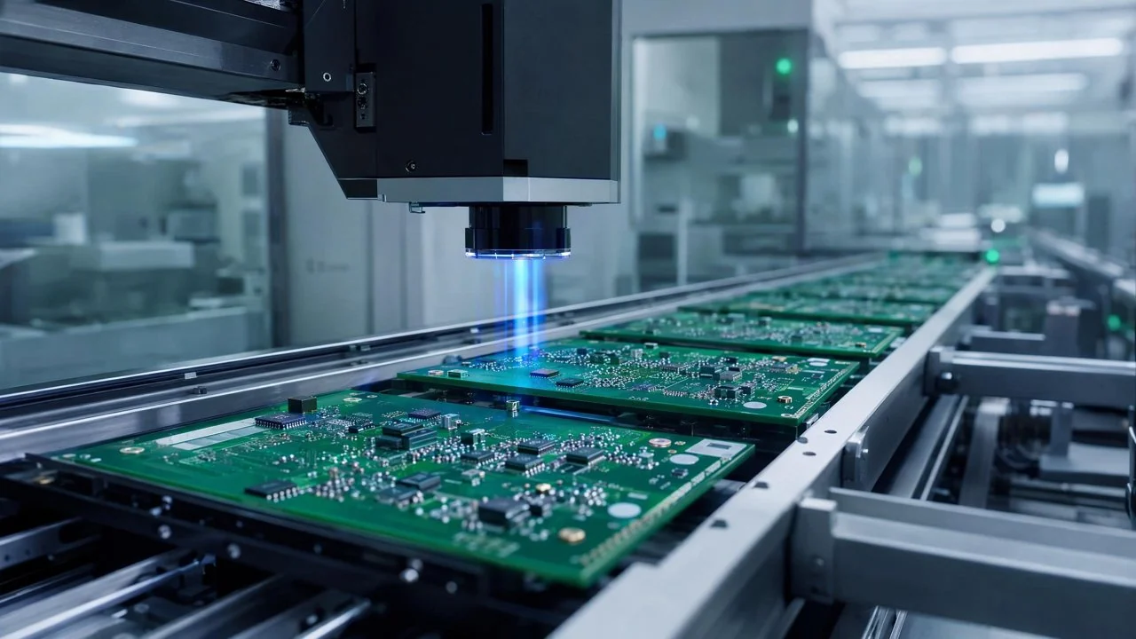
In the electronics manufacturing sector, the quality of SMT (Surface Mount Technology) solder joints is critical to the reliability of PCBA (Printed Circuit Board Assembly). DaoAI 2D ACI equipment (high-resolution 2D imaging + deep learning secondary judgment, targeting surface/printing/character OCR/assembly defects, high-speed online full inspection, micron-level, semantic false positive filtering) precisely identifies solder joint defects such as open circuits, bridging, and insufficient solder, and filters semantic false positives, reducing the false positive rate on a leading electronics manufacturer's production line from 1.8% to 0.68%, while decreasing manual re-inspection hours by 45%. This not only significantly improves inspection efficiency and accuracy but also effectively mitigates the secondary labor costs and production line stoppage risks associated with the high false positive rates of traditional AOI.
DaoAI 2D ACI equipment (high-resolution 2D imaging + deep learning secondary judgment, targeting surface/printing/character OCR/assembly defects, high-speed online full inspection, micron-level, semantic false positive filtering) precisely identifies solder joint defects such as open circuits, bridging, and insufficient solder, and filters semantic false positives, reducing the false positive rate on a leading electronics manufacturer's production line from 1.8% to 0.68%, while decreasing manual re-inspection hours by 45%. In the electronics industry, particularly PCBA manufacturing, product quality and reliability are paramount. After SMT placement, solder joint quality directly determines the functional stability and lifespan of the circuit board. Open circuits, bridging, and insufficient solder are the most common and damaging types of SMT solder joint defects, potentially leading to open circuits, short circuits, or poor contact. As electronic products become smaller and more integrated, component spacing shrinks, and pad sizes continuously decrease, making solder joint defect detection exponentially more challenging. A tier-1 supplier specializing in high-end consumer electronics and industrial control modules, with a daily output of tens of thousands of PCBAs on its SMT production line, has stringent requirements for solder joint inspection accuracy and efficiency. Traditional Automated Optical Inspection (AOI) equipment has shown limitations in this area, especially when dealing with complex solder joint morphologies and subtle defects, struggling to balance low false negative rates with low false positive rates, thus becoming a bottleneck for quality and efficiency improvements on the production line.
Pain Points: Why This Hurdle Is Difficult to Overcome
The challenges faced by this leading supplier are multifaceted. Firstly, high false positive rates, averaging 1.8%, led to significant human resources being dedicated daily to secondary re-inspection, substantially increasing operational costs and manual re-inspection hours (accounting for approximately 35% of total inspection man-hours). Secondly, for some subtle defects with blurry edges or similar colors (e.g., slight open circuits, solder balls), the false negative rate of traditional rule-based AOI remained around 0.4%, posing potential product quality risks and compliance pressures. Furthermore, due to the large number of product models, traditional AOI required at least 30 minutes for program debugging and parameter adjustment during each line changeover, severely impacting production rhythm and equipment utilization.
The root cause of these difficulties lies in the inherent complexity of SMT solder joint inspection. From a process perspective, the morphology of solder joints formed during reflow soldering is influenced by various factors such as solder paste composition, reflow profile, and component lead solderability. Even good products exhibit a certain degree of variation in appearance. The objective existence of such 'imperfect good products' makes traditional rule-based AOI highly prone to false positives. From an imaging perspective, solder joint surfaces often have reflections, shadows, and interferences like solder paste residue and flux marks. While high-resolution 2D imaging can capture details, effectively distinguishing these interferences from true defects is a technical challenge. Moreover, the current trend in industrial robot collision detection technology, shifting from early mechanical modeling to adaptive control, precisely addresses the challenges of 'uncertainty' and 'complexity' in industrial scenarios. Analogously in the AOI field, solder joint inspection also needs to transition from static rule matching to dynamic, self-learning, and adaptive intelligent discrimination to cope with ever-changing production environments and increasingly complex defect patterns.
Technical Principles
The core competitiveness of DaoAI 2D ACI equipment lies in its innovative mechanism combining high-resolution 2D imaging with deep learning for secondary judgment. The equipment utilizes industrial-grade high-resolution cameras, coupled with multi-angle annular lighting, to acquire clear, shadow-free image data of the solder joint area, ensuring micron-level defect features are fully captured. After image acquisition, unlike traditional AOI which relies on engineers manually writing rule libraries (e.g., area, perimeter, grayscale thresholds), the DaoAI system incorporates an AI judgment module based on advanced deep learning algorithms. This module first pre-trains on vast amounts of solder joint images using a visual foundation model, giving it the ability to recognize basic solder joint features. For specific production lines and products, the system employs APDT (Active Positive Data Training) few-shot learning technology, requiring only 1–20 good product images to quickly establish a judgment model. This model learns and understands the subtle morphological variations of good solder joints, enabling more precise identification of various defects such as open circuits, bridging, and insufficient solder. More importantly, the system's built-in semantic false positive filtering mechanism can distinguish between 'acceptable deviations' caused by process fluctuations or normal surface traces and true defects, significantly reducing false positive rates.
Compared to traditional rule-based AOI, DaoAI 2D ACI offers several advantages: Firstly, traditional rule-based AOI faces high costs for rule writing and maintenance when dealing with complex and varied solder joint morphologies, and struggles to cover all abnormal situations, often leading to false negatives or false positives. ACI, on the other hand, automatically extracts features and patterns from data through deep learning, eliminating the need for manual rule intervention, and possesses stronger generalization and robustness. Secondly, manual visual inspection, while flexible to some extent, is inefficient, susceptible to subjective factors, and costly, making it unsuitable for high-speed online full inspection requirements. DaoAI equipment can perform high-speed online full inspection, ensuring the quality of every PCBA solder joint, while AI-assisted judgment significantly reduces the burden of manual re-inspection. Furthermore, its 'one good product, 5-minute, 0-code automatic programming' feature greatly shortens changeover time and enhances production line flexibility.
Typical Application Scenarios
- **SMT Solder Joint Open Circuit Detection:** Detecting whether an effective connection is formed between the solder pad and component lead, and if there are voids, cracks, or poor wetting. The difficulty lies in that open circuits may manifest as very subtle gaps or incomplete wetting, which are challenging for traditional methods to consistently capture.
- **SMT Solder Joint Bridging Detection:** Identifying whether there are unwanted solder bridges between adjacent solder joints, which can cause short circuits. The difficulty arises as component spacing shrinks, tiny solder bridges can be easily overlooked under complex lighting, and may be confused with solder balls.
- **SMT Solder Joint Insufficient Solder Detection:** Determining if the solder volume is adequate, if the solder joint is full, and if there is collapse or insufficient solder. The difficulty lies in the flexibility of the criteria for insufficient solder, and the solder joint's edge contours may be irregular, easily confused with normal morphology.
- **SMT Component Misalignment/Skew Detection:** Checking if the placed components are accurately positioned on the pads, and if there is offset or rotation. The difficulty is that minor misalignments may not affect functionality, but could lead to reliability issues over time, requiring high-precision positioning and comparison.
- **SMT Character OCR Recognition:** Performing optical character recognition and verification for silkscreen characters, batch numbers, serial numbers, etc., on PCBAs. The difficulty is that characters may be blurry or deformed due to printing quality, background textures, uneven lighting, affecting recognition accuracy.
Case Study
A leading Tier-1 electronics manufacturing service provider, whose factory in South China primarily produces communication modules and high-end industrial control boards, has extremely high reliability requirements for its products. Before introducing DaoAI 2D ACI equipment, solder joint inspection at this factory relied mainly on traditional AOI equipment and extensive manual re-inspection. The false positive rate of traditional AOI consistently hovered around 1.8%, necessitating the deployment of 8-10 skilled workers for several hours daily to ensure outgoing quality. Furthermore, due to the wide variety of products, traditional AOI program adjustments typically took 30-45 minutes during each line changeover, severely restricting production efficiency. After thorough research and rigorous testing, the manufacturer decided to deploy DaoAI 2D ACI equipment. In the initial deployment phase, our technical team collaborated closely with the client's engineers, utilizing a small amount of good product data provided by the client for model training and optimization. Through APDT positive sample learning, a new product model's inspection program was programmed in just 5 minutes using only 15 good product images. After three months of stable operation, at the manufacturer's site, data showed that the DaoAI equipment not only improved solder joint defect detection rates to 99.4% (corresponding to a false negative rate of less than 0.6%) but, more importantly, significantly reduced the false positive rate to 0.68%, a substantial improvement of 62%. This directly resulted in a 45% reduction in manual re-inspection hours, freeing up significant human resources. Concurrently, changeover time was shortened to 5 minutes, greatly enhancing production line flexibility and equipment utilization.
“The introduction of DaoAI's ACI equipment has completely transformed the efficiency and accuracy of solder joint inspection on our production line. The significant reduction in false positives not only saved us labor costs but also allowed engineers to focus on more valuable process optimization work.”
The figures above are a typically achievable range in anonymized industry scenarios — a different line or a different batch of parts will move the result either way; on-site measurement governs.
DaoAI Solutions and Products
The core solution provided by DaoAI to this client was based on the DaoAI 2D ACI equipment. This equipment integrates a high-resolution optical imaging module and a high-performance computing platform, powered by the DaoAI ACI OS. During implementation, we first conducted a detailed assessment of the client's existing production line to ensure smooth integration of the equipment into their SMT production process. In the modeling phase, utilizing the DaoAI ACI OS's 'one good product, 5-minute, 0-code automatic programming' feature, client engineers could quickly establish inspection models for new products without needing specialized AI programming knowledge. The system's APDT positive sample/few-shot learning mechanism requires only a small number of good product images for model training, greatly shortening the deployment cycle. For complex and varied solder joint defects, the system's built-in semantic false positive filtering function effectively distinguishes between normal variations caused by process fluctuations and true defects, significantly reducing the false positive rate. Furthermore, DaoAI offers flexible deployment options, supporting SDK/API/Docker forms, and enables 100% local private deployment, ensuring client data security remains in-house. While this case primarily focuses on 2D ACI, other DaoAI product lines, such as DaoAI 3D ACI equipment (for hidden solder joints and 3D morphology inspection) and DaoAI Robot Vision (for bin picking and assembly guidance), can also be expanded and integrated based on future client needs to build more comprehensive intelligent manufacturing solutions.
Through the successful deployment of DaoAI 2D ACI equipment, the client achieved significant quantifiable results. In terms of quality, the detection rate for solder joint defects consistently exceeded 99.4%, with a false negative rate below 0.6%, effectively avoiding potential product quality risks. In terms of efficiency, the false positive rate was reduced by 62%, leading to a 45% reduction in manual re-inspection hours, greatly improving the automation level of the inspection process and production rhythm. Concurrently, changeover time was shortened from the original 30-45 minutes to less than 5 minutes, significantly enhancing production line flexibility and equipment utilization. These improvements directly translated into lower manufacturing costs, faster market response times, and higher customer satisfaction, demonstrating the immense value of AI vision inspection in modern electronics manufacturing.
FAQ
How does DaoAI 2D ACI equipment handle reflections and shadows on solder joint surfaces?
Our equipment employs a multi-angle annular lighting design, combined with advanced image processing algorithms, to effectively suppress reflections and shadows on solder joint surfaces, generating uniform and high-contrast images. This ensures that the AI model can accurately extract defect features from clear image data, avoiding misjudgments caused by uneven lighting.
How long does it take to program the inspection process for new product models on the ACI equipment?
DaoAI 2D ACI equipment boasts a 'one good product, 5-minute, 0-code automatic programming' capability. Leveraging APDT positive/few-shot learning technology, clients only need to provide 1–20 good product images, and the system can automatically complete model training and inspection program setup within minutes, significantly reducing changeover and deployment time.
How does DaoAI ACI equipment distinguish between 'good product deviations' caused by process fluctuations and actual defects?
This is due to our deep learning model's powerful feature learning capabilities and semantic false positive filtering mechanism. During training, the model learns the subtle morphological variations of numerous good solder joints, understanding their normal fluctuation range. When an area with subtle differences from good product features, but not meeting defect criteria, is detected, the semantic false positive filtering mechanism identifies it as a 'good product deviation' rather than a defect, thereby significantly reducing the false positive rate.
Full solution for this scenario: the full inspection solution for Electronics / PCBA
This article was generated by AI. Customer cases are simulated scenarios based on real product capabilities and figures are illustrative; see product pages for official benchmarks.