
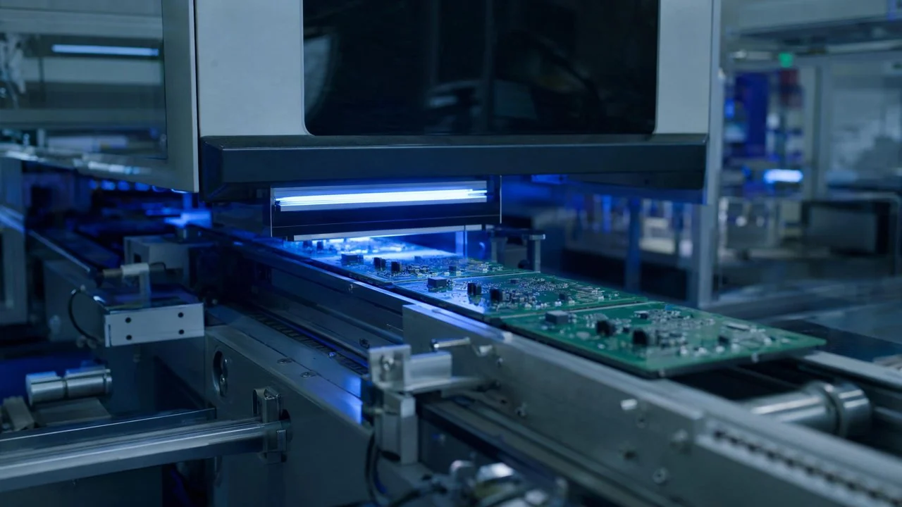
In the electronics/PCBA industry, the quality detection of SMT solder joints is crucial. WeLinkirt's 2D ACI equipment provides an effective solution for solder joint defect detection with advanced technology.
In recent years, the electronics/PCBA industry has developed rapidly, with electronic products continuously moving towards miniaturization and high-performance. On the SMT (Surface Mount Technology) production line, the quality of SMT solder joints directly affects the performance and reliability of electronic products. An electronics manufacturing enterprise's SMT production line mainly produces various types of PCB boards, and its detection targets are defects such as cold solder joints, solder bridging, and insufficient solder in SMT solder joints. These solder joints are tiny and densely packed, making it difficult for traditional detection methods to meet the requirements of high-precision and high-efficiency detection.
Pain Points: Why Is It So Difficult to Overcome?
From multiple dimensions, the enterprise faces many difficulties. In terms of the false-negative rate, the false-negative rate of traditional rule-based AOI for complex solder joint defects is as high as 4%, resulting in some defective products flowing into subsequent processes. The false-positive rate is even more serious, reaching 20%. A large number of false positives require manual re-judgment, increasing the manual re-judgment working hours. On average, the manual re-judgment working hours per day reach 8 hours. The long downtime for model change is also a major problem. Each model change requires a 2-hour downtime for parameter adjustment, affecting production efficiency. From the perspective of compliance risks, if solder joint defects are not detected in time, the product quality may fail to meet the standards, facing risks such as market recalls, which increases the single-piece cost.
The reason these problems are difficult to solve is as follows. From the process level, the soldering process of SMT solder joints is complex. Different soldering parameters result in different solder joint shapes, making it difficult to use unified rules for detection. From the imaging level, tiny solder joints are difficult to image clearly under traditional imaging equipment, limiting the detection accuracy. From the material level, different solders and PCB materials affect the appearance and electrical performance of solder joints, increasing the difficulty of defect detection. Combining with today's hot-topic direction, the performance of domestic world models adapted to domestic Ascend computing power in industrial vision quality inspection scenarios remains to be verified, and traditional detection methods are difficult to fully utilize this new computing-power advantage.
Technical Principle
WeLinkirt's 2D ACI equipment uses high-resolution 2D imaging technology to clearly capture the subtle features of solder joints. At the same time, it combines the deep-learning secondary image-judgment algorithm. Through a large amount of solder joint data for training, the model learns the normal and defective features of solder joints. The hardware mechanism of the equipment includes a high-performance industrial camera and a stable light source system to ensure the clarity and stability of imaging. This method is effective because the deep-learning algorithm can automatically learn and identify complex solder joint features, not limited by traditional rules, and can more accurately detect various solder joint defects.
Compared with traditional rule-based AOI, rule-based AOI requires manual setting of complex detection rules and is difficult to adapt to the diversity of solder joint shapes. In contrast, the 2D ACI equipment can automatically learn through deep learning and quickly adapt to different solder joints and defect types. Compared with manual visual inspection, manual visual inspection is easily affected by fatigue and subjective factors, with low detection efficiency and accuracy. The 2D ACI equipment can achieve high-speed online full-inspection, improving detection efficiency and accuracy.
Typical Application Scenarios
- Cold solder joint detection: High-resolution 2D imaging is used to capture the shape and texture features of solder joints. The deep-learning algorithm analyzes the connection between the solder joint and the PCB board to determine whether there is a cold solder joint. The difficulty lies in the fact that the features of cold solder joints are not obvious, and the algorithm needs to have high sensitivity and accuracy.
- Solder bridging detection: The equipment accurately images the edges and contours of solder joints to identify whether there is a connection between adjacent solder joints. The difficulty lies in the various shapes of solder bridging, which may be similar to the edge features of normal solder joints, easily leading to false judgments.
- Insufficient solder detection: The area and height of the solder joint are analyzed to determine whether the solder volume of the solder joint is sufficient. The difficulty lies in the different degrees of insufficient solder, and the algorithm needs to accurately distinguish between normal and insufficient-solder joints.
- Surface defect detection: Defects such as scratches and cracks on the surface of solder joints are detected. High-resolution imaging and deep learning are used to analyze the surface features. The difficulty lies in the fact that surface defects are tiny, requiring high-resolution imaging equipment and a delicate algorithm.
Implementation Case
A medium-sized electronics manufacturing enterprise produces 5000 PCB boards per day on its SMT production line. Before introducing WeLinkirt's 2D ACI equipment, the false-negative rate was 4%, the false-positive rate was 20%, and the downtime for model change was 2 hours. During the implementation process, WeLinkirt's technical team installed and debugged the equipment, used 10 good-quality samples for positive-sample learning, and quickly completed the modeling. After the implementation, the false-negative rate was reduced to 0.6%, the false-positive rate was reduced to 5%, and the downtime for model change was shortened to 5 minutes.
The 2D ACI equipment brings a high-precision and high-efficiency solution for SMT solder joint detection.
WeLinkirt's Solution and Product
Centered on the 2D ACI equipment, WeLinkirt provides a complete solution. In terms of modeling, the DaoAI ACI OS is used. Through positive-sample/less-sample learning with 1-20 good-quality samples, zero-code automatic programming for a good-quality product can be completed in 5 minutes. In terms of model change, the equipment can quickly adapt to different products and processes, and the model-change time is shortened to 5 minutes. In terms of deployment, it supports 100% local privatization, ensuring data security with data remaining within the factory. At the same time, it can be integrated with the enterprise's existing production-line system for smooth docking.
By using WeLinkirt's 2D ACI equipment, the enterprise has achieved remarkable results in many aspects. In terms of detection accuracy, the detection rate has reached 99.4%, greatly improving the product quality. The false-positive rate has been reduced by 75%, reducing the manual re-judgment working hours and improving production efficiency. The model-change time has been shortened from 2 hours to 5 minutes, reducing the downtime and increasing the production capacity.
FAQ
What is the accuracy of the 2D ACI equipment in detecting SMT solder joints?
The 2D ACI equipment has high accuracy in detecting SMT solder joints, with a detection rate of up to 99.4%. It uses high-resolution 2D imaging and deep-learning algorithms to clearly capture the subtle features of solder joints and accurately identify various defects such as cold solder joints and solder bridging, far exceeding traditional detection methods.
How long does it take for the equipment to change models?
It only takes 5 minutes for the 2D ACI equipment to change models. With the DaoAI ACI OS, positive-sample/less-sample learning can be carried out with 1-20 good-quality samples to quickly complete the modeling and adapt to different products and processes.
How much can the equipment reduce the false-positive rate?
The equipment can effectively reduce the false-positive rate. Compared with traditional methods, the false-positive rate is reduced by 75%. The deep-learning secondary image-judgment algorithm can accurately distinguish between normal and defective solder joints, reducing unnecessary false judgments and the workload of manual re-judgment.
Full solution for this scenario: Electronics / PCBA industry solutions
This article was generated by AI. Customer cases are simulated scenarios based on real product capabilities and figures are illustrative; see product pages for official benchmarks.