
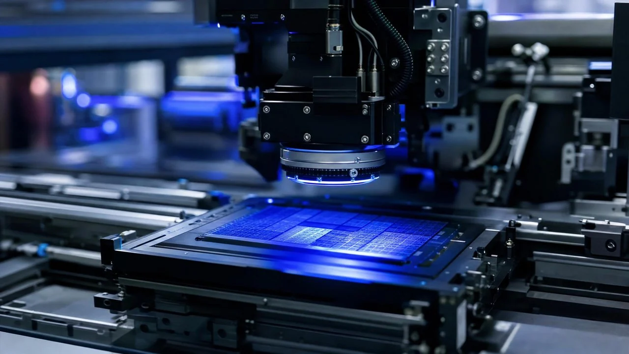
In the field of semiconductor chip production, the detection of chip pin coplanarity and dicing chipping is a crucial step to ensure product quality. WeLinkirt's 3D ACI equipment brings a more precise and efficient detection solution to the industry with its advanced technology.
Industry Background and User Scenario: Semiconductor chips, as the core components of modern electronic devices, involve numerous complex processes in their production, with extremely high requirements for quality control. In the chip packaging production line, the pin welding and dicing processes are crucial. A leading semiconductor chip manufacturer focuses on the production of high-performance semiconductor chips, which are widely used in smartphones, computers, automotive electronics and other fields. During the production process, the manufacturer needs to strictly detect the pin coplanarity and dicing chipping of the chips to ensure that the products meet high-quality standards and prevent defective products from entering the market.
Pain Points: Why Is It Difficult?
Under the current trend of industrial vision quality inspection applications with domestic GPU direct-access solutions, the manufacturer faces many difficulties. Quantitatively, the false-negative rate of traditional detection methods is as high as 3%, which means that 3 out of every 100 chips may have defective products flowing into subsequent processes. These defective products may lead to a decline in the performance of the entire product, increasing production risks and costs. For example, in mobile phone chips, if there are problems with pin coplanarity, it may affect the signal transmission and stability of the mobile phone. At the same time, the false-positive rate reaches 15%, and a large number of good products are misjudged as defective products. This not only increases the re-inspection workload but also leads to a significant increase in labor costs. According to statistics, due to misjudgment, the manufacturer needs to invest a large amount of additional labor for re-inspection every month. In addition, the model change time is as long as 30 minutes. In the face of rapidly changing market demands, this inefficient model change method seriously affects production efficiency and is difficult to meet the production requirements of rapid model change.
The root cause of these problems lies in the limitations of traditional detection methods. Traditional 2D optical detection technology can only obtain two-dimensional information on the chip surface and cannot comprehensively present the three-dimensional features of the chip. For defects in 2D optical blind areas such as hidden solder joints, coplanarity, micron-level topography, and air holes, traditional methods are difficult to detect accurately. Moreover, traditional detection algorithms have limited recognition ability for complex chip surface features, which is prone to misjudgment and false-negative situations. In addition, the model change process of traditional equipment is complex, requiring a large amount of manual parameter setting and adjustment, resulting in a long model change time.
Technical Principle
WeLinkirt's 3D ACI equipment uses a self-developed 3D camera for image acquisition. The camera has the characteristics of high resolution and high precision, and can collect clear and accurate chip image data. Through the three-dimensional topography reconstruction technology, the collected 2D image data is converted into 3D point cloud data, providing more comprehensive information for defect detection. The equipment uses advanced algorithms to analyze the three-dimensional topography of the chip and can accurately identify defects in 2D optical blind areas such as hidden solder joints, coplanarity, micron-level topography, and air holes.
Compared with traditional 2D imaging, 3D imaging can obtain the three-dimensional information of the chip and present the surface features of the chip more comprehensively. For example, for the detection of pin coplanarity, 3D point cloud data can accurately measure the height and position of each pin and compare it with the standard value to accurately determine whether the pins are coplanar. While 2D imaging can only see the planar image of the pins and cannot accurately judge the height and coplanarity of the pins. For the detection of dicing chipping, 3D imaging can clearly capture the tiny defects on the dicing edge and avoid false-negatives. While 2D imaging may miss some tiny defects due to the perspective problem. In addition, the equipment also uses 2D-3D fusion technology, combining the texture information of 2D images and the three-dimensional information of 3D point clouds to further improve the detection accuracy.
Typical Application Scenarios
- Pin Coplanarity Detection: In the chip packaging process, the coplanarity of pins directly affects the connection quality between the chip and the circuit board. WeLinkirt's 3D ACI equipment accurately measures the height and position of each pin through 3D point cloud data and compares it with the standard value. The difficulty lies in the large number of pins and the small spacing, which requires high-precision measurement and analysis algorithms.
- Dicing Chipping Detection: In the dicing process, chipping defects are prone to occur on the dicing edge. The equipment uses 3D imaging technology to clearly capture the tiny defects on the dicing edge. The difficulty lies in that the chipping defects are usually very small, which requires a high-resolution camera and a sensitive detection algorithm.
- Hidden Solder Joint Detection: Hidden solder joints inside the chip are difficult to find through 2D optical detection. The 3D ACI equipment can accurately identify the defects of hidden solder joints through three-dimensional topography reconstruction and advanced algorithms. The difficulty lies in that the hidden solder joints are located inside the chip, and information needs to be obtained by penetrating the chip surface.
- Micron-Level Topography Detection: Micron-level topography defects on the chip surface may affect the performance of the chip. The equipment can detect these tiny topography defects through a high-precision 3D camera and algorithms. The difficulty lies in that micron-level defects are very difficult to detect, which requires extremely high resolution and sensitivity.
- Air Hole Detection: Air holes inside the chip may affect the heat dissipation and electrical performance of the chip. The 3D ACI equipment can detect the existence and size of air holes by analyzing 3D point cloud data. The difficulty lies in that air holes are usually hidden inside the chip, which requires accurate three-dimensional imaging and analysis technology.
Implementation Case
A leading semiconductor chip manufacturer has a large-scale chip packaging production line. Before introducing WeLinkirt's 3D ACI equipment, the manufacturer faced problems such as high false-negative rate, high false-positive rate, and long model change time. During the implementation process, WeLinkirt's technical team installed and debugged the equipment and trained the operators. After a period of trial operation, the equipment gradually ran stably. Before the implementation, the false-negative rate of chip pin coplanarity and dicing chipping was 3%, the false-positive rate was 15%, and the model change time was 30 minutes. After the implementation, the detection rate increased to 98.5%, the false-negative rate decreased to <1.5%, the false-positive rate decreased by 68%, and the model change time was shortened to 5 minutes.
WeLinkirt's 3D ACI equipment has brought a qualitative leap to semiconductor chip detection, significantly improving detection efficiency and accuracy.
WeLinkirt's Solution and Products
Centered on the 3D ACI equipment, WeLinkirt provides a complete detection solution for the manufacturer. The equipment can quickly and accurately detect the pin coplanarity and dicing chipping of the chips. The supporting DaoAI ACI OS can realize the feature recognition of the visual basic model. Only one good product is needed, and 0-code automatic programming can be completed in 5 minutes. Through APDT positive sample/few-sample learning (only 1-20 good products are needed), the programming time and sample requirements are effectively reduced. At the same time, the semantic false-positive filtering function can reduce the false-positive rate. In the actual implementation process, the equipment is installed on the chip packaging production line. Through real-time detection of the chips, the detection results are timely fed back to the production system for timely processing of defective products.
Quantitative Results: After using WeLinkirt's 3D ACI equipment, the detection rate of chip pin coplanarity and dicing chipping increased to 98.5%, and the false-negative rate decreased to <1.5%. The false-positive rate decreased by 68%, significantly reducing the re-inspection workload. The model change time was shortened to 5 minutes, greatly improving production efficiency and better meeting the production requirements of rapid model change.
FAQ
What chip defects can the 3D ACI equipment detect?
The equipment can detect defects such as hidden solder joints, coplanarity, micron-level topography, and air holes. It is especially good at detecting defects in 2D optical blind areas such as chip pin coplanarity and dicing chipping, with a detection rate of 98.5%. Through 3D imaging and advanced algorithms, it can more comprehensively and accurately find various potential problems of the chips.
How much can the false-positive rate be reduced by WeLinkirt's solution?
After using the solution, the false-positive rate is reduced by 68%, significantly reducing the re-inspection workload and improving production efficiency. The semantic false-positive filtering function of the supporting DaoAI ACI OS plays a key role in effectively identifying and filtering out misjudgment information.
How short can the model change time be shortened to?
The model change time can be shortened to 5 minutes, which can better meet the production requirements of rapid model change and improve the flexibility and efficiency of production. This benefits from the 0-code automatic programming and APDT positive sample/few-sample learning technology of the equipment, reducing the parameter setting and adjustment time during model change.
Full solution for this scenario: Semiconductor / chips industry solutions · Lithography Pattern Defect Detection
This article was generated by AI. Customer cases are simulated scenarios based on real product capabilities and figures are illustrative; see product pages for official benchmarks.