
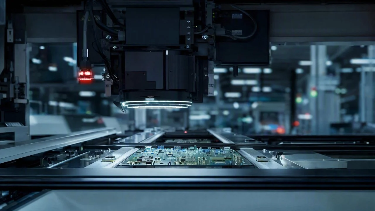
Wemio's 3D ACI equipment (self-developed 3D camera + three-dimensional morphology reconstruction/point cloud, detecting hidden solder joints, coplanarity, micron-level morphology, air holes and other 2D optical blind-spot defects, 2D-3D fusion), through high-precision detection algorithms and advanced imaging technology, has reduced the missed detection rate of manual visual inspection from 5% to less than 1%. In the electronics/PCBA industry, with the continuous improvement of the miniaturization and integration of electronic products, the components on circuit boards have become more dense, and the soldering process has become more complex. A certain electronics manufacturer's production line mainly produces various printed circuit boards (PCBA). The inspection objects include BGA packages, QFN packages, etc. These packaged components are prone to hidden solder joints, air holes and other defects during the soldering process, and traditional manual visual inspection is difficult to meet the inspection requirements.
Industry background and user scenario: With the rapid development of the electronics/PCBA industry, the quality requirements for products are getting higher and higher. In the production process of circuit boards, the inspection link is crucial as it is directly related to the reliability and stability of products. The traditional manual visual inspection method is not only inefficient but also easily affected by human factors, leading to missed detections and misjudgments. Wemio's 3D ACI equipment emerged as the times require. It uses a self-developed 3D camera and three-dimensional morphology reconstruction/point cloud technology to detect hidden solder joints, coplanarity, micron-level morphology, air holes and other 2D optical blind-spot defects, and realizes 2D-3D fusion detection, providing a high-precision and high-efficiency inspection solution for the electronics/PCBA industry.
Pain points: Why is this hurdle so difficult to cross?
Multi-dimensional quantification of pain points: Manual visual inspection faces many difficulties in the electronics/PCBA industry. First of all, the missed detection rate is relatively high, reaching about 5% on average. Due to the easy fatigue of manual workers during long-term work, it is difficult to accurately identify some subtle defects. Secondly, the false alarm rate cannot be underestimated, about 8%. The subjectivity of manual judgment is relatively large, and normal situations are easily misjudged as defects. Moreover, the manual re-judgment working hours are too long. A large amount of time is required to confirm each suspected defect, resulting in low production efficiency. In addition, the labor cost of manual visual inspection is high. With the continuous rise of labor costs, the burden on enterprises is increasing. At the same time, the change-over downtime is long. When the production line changes the product model, manual visual inspection requires retraining and adjustment, resulting in an increase in downtime and affecting the production progress.
Root cause analysis: From the process level, the packaging technology of modern electronic components is constantly improving, such as BGA packaging and QFN packaging. The solder joints of these packages are hidden under the components, and traditional 2D optical detection cannot see them, let alone manual visual inspection. From the imaging level, 2D imaging can only provide planar information, and it is difficult to accurately judge some three-dimensional defects such as air holes and coplanarity problems. From the material level, the new materials used on the circuit boards may affect the reflection and refraction of light, making manual visual inspection more difficult. From the rhythm level, the production rhythm of the electronics/PCBA industry is getting faster and faster, and the speed of manual visual inspection cannot meet the rhythm requirements of the production line. Combined with the application prospect of the world's first industrial multi-modal large model, the traditional manual visual inspection method can no longer meet the development needs of the industry.
Technical principle
In-depth mechanism: Wemio's 3D ACI equipment uses a self-developed 3D camera to obtain the three-dimensional morphology information of the circuit board. Through three-dimensional morphology reconstruction and point cloud technology, the obtained three-dimensional data is processed and analyzed to construct an accurate three-dimensional model of the circuit board. During the inspection process, the equipment compares the actual three-dimensional model with the pre-set standard model, and uses advanced algorithms to identify defects such as hidden solder joints, coplanarity, micron-level morphology, and air holes. For example, for hidden solder joints, the equipment can judge whether there are defects by analyzing the three-dimensional morphology changes around the solder joints; for air holes, the equipment can accurately identify the size, shape, and position of the air holes based on the three-dimensional model.
Comparison with traditional methods: Compared with traditional rule-based AOI, Wemio's 3D ACI equipment has stronger adaptability and flexibility. Rule-based AOI detects based on preset rules and may not be able to accurately detect some complex defects and new products. The 3D ACI equipment can continuously learn and optimize through deep learning algorithms to adapt to different types of products and defects. Compared with manual visual inspection, the 3D ACI equipment has higher detection accuracy. The missed detection rate can be reduced to less than 1%, and the false alarm rate can be reduced to less than 3%, greatly improving the detection efficiency and quality. At the same time, the detection speed of the equipment is fast, which can meet the rhythm requirements of the production line, reducing manual re-judgment working hours and labor costs.
Typical application scenarios
- BGA package inspection: The solder joints of BGA packages are hidden under the components, which is a blind spot for 2D optical detection. Wemio's 3D ACI equipment can clearly see the situation of the solder joints through three-dimensional morphology reconstruction and point cloud technology, and detect defects such as false soldering and short-circuits of the solder joints. The difficulty lies in the small and hidden solder joints, which require high-precision imaging and analysis algorithms.
- QFN package inspection: The soldering area between the pins of QFN packages and the circuit board is prone to coplanarity problems and air hole defects. The equipment can judge whether the coplanarity meets the requirements by detecting the three-dimensional morphology and height information of the pins, and accurately identify the size and position of the air holes at the same time. The difficulty lies in the precise measurement of tiny air holes and coplanarity.
- Chip component inspection: Chip components may have problems such as offset and tombstoning during the soldering process. The 3D ACI equipment can detect these defects in time by analyzing the three-dimensional position and attitude information of the components. The difficulty lies in the accurate identification of small offsets and attitude changes of the components.
- Printed circuit board inspection: There may be defects such as short-circuits, open-circuits, and burrs in the circuits and pads on the printed circuit board. The equipment can detect these potential problems by detecting the three-dimensional morphology of the circuit board. The difficulty lies in the detection of complex circuits and tiny defects.
Implementation case
Comparison before and after the implementation of an anonymous customer: A medium-sized electronics manufacturer mainly produces various PCBA products. Before introducing Wemio's 3D ACI equipment, the manufacturer used manual visual inspection, with a missed detection rate of about 5% and a false alarm rate of about 8%. The manual re-judgment working hours were long, and the labor cost was high. After the implementation of the 3D ACI equipment, the missed detection rate was reduced to 0.8%, the false alarm rate was reduced to 2%, the manual re-judgment working hours were reduced by 70%, and the labor cost was reduced by 40%. At the same time, the change-over downtime was shortened from the original 30 minutes to 5 minutes, greatly improving the production efficiency.
Wemio's 3D ACI equipment has brought significant benefits to electronics manufacturers and is an ideal choice for inspection in the electronics/PCBA industry.
Wemio's solution and product
Product capabilities and implementation methods: Wemio's 3D ACI equipment is centered on its powerful detection capabilities and advanced technology. In terms of modeling, the equipment can automatically program with zero code in 5 minutes using one good product, and combine APDT positive sample/few-shot learning (1-20 good products) to quickly establish an accurate detection model. In terms of change-over, the change-over time of the equipment is only 5 minutes, greatly shortening the downtime of the production line. In terms of deployment, it supports various deployment methods such as SDK/API/Docker, and can achieve 100% local private deployment to ensure data security. In terms of integration, the equipment can be integrated with other equipment on the production line to achieve automated inspection. In addition, Wemio also has a supporting DaoAI ACI OS that can perform feature recognition of the visual basic model and semantic false alarm filtering to further improve the accuracy of detection.
Quantitative results and business value: By using Wemio's 3D ACI equipment, enterprises have achieved remarkable results in many aspects. The missed detection rate has been reduced to 0.8%, greatly improving the quality and reliability of products. The false alarm rate has been reduced to 2%, reducing unnecessary manual re-judgment and improving production efficiency. The manual re-judgment working hours have been reduced by 70%, and the labor cost has been reduced by 40%, saving a large amount of labor cost for the enterprise. The change-over downtime has been shortened to 5 minutes, improving the utilization rate of the production line and increasing the enterprise's production capacity. At the same time, the high-precision detection capability of the equipment helps enterprises improve their brand image and enhance their market competitiveness.
FAQ
What is the 3D ACI equipment?
The 3D ACI equipment is an advanced inspection device developed by Wemio. It uses a self-developed 3D camera and three-dimensional morphology reconstruction/point cloud technology to detect hidden solder joints, coplanarity and other 2D optical blind-spot defects, realizing 2D-3D fusion detection and improving inspection accuracy and efficiency.
How to choose between the 3D ACI equipment and traditional AOI equipment?
Traditional AOI is based on preset rules and has limited detection capabilities for complex defects and new products. Wemio's 3D ACI equipment can adapt to different products and defects through deep learning, with higher detection accuracy and lower false alarm and missed detection rates, which is suitable for scenarios with high-quality requirements.
How much does it cost to use the 3D ACI equipment?
The quotation of the 3D ACI equipment is affected by factors such as equipment model, functional configuration, and detection requirements. If you want to get a specific quotation, you can contact Wemio for an appointment, and we will provide a detailed solution and price.
Full solution for this scenario: Electronics / PCBA industry solutions
This article was generated by AI. Customer cases are simulated scenarios based on real product capabilities and figures are illustrative; see product pages for official benchmarks.